Method of etching silicon

a silicon and etching technology, applied in the field of etching silicon, can solve the problems of reducing affecting the performance of the end product, and quickly outweighing the savings in material costs

Inactive Publication Date: 2006-12-28
CSG SOLAR AG
View PDF14 Cites 25 Cited by
  • Summary
  • Abstract
  • Description
  • Claims
  • Application Information

AI Technical Summary

Benefits of technology

[0006] c) Applying a dilute solution of hydrofluoric acid (HF) and potassium permanganate (KMnO4)

Problems solved by technology

However in practice cost savings have been difficult to achieve as a major component of cost is the number and complexity of process steps involved in the manufacturing sequence and can quickly outweigh savings in material costs.
In particular the number of steps that require precise alig

Method used


Image

  • Method of etching silicon
  • Method of etching silicon
  • Method of etching silicon

Examples


Embodiment Construction

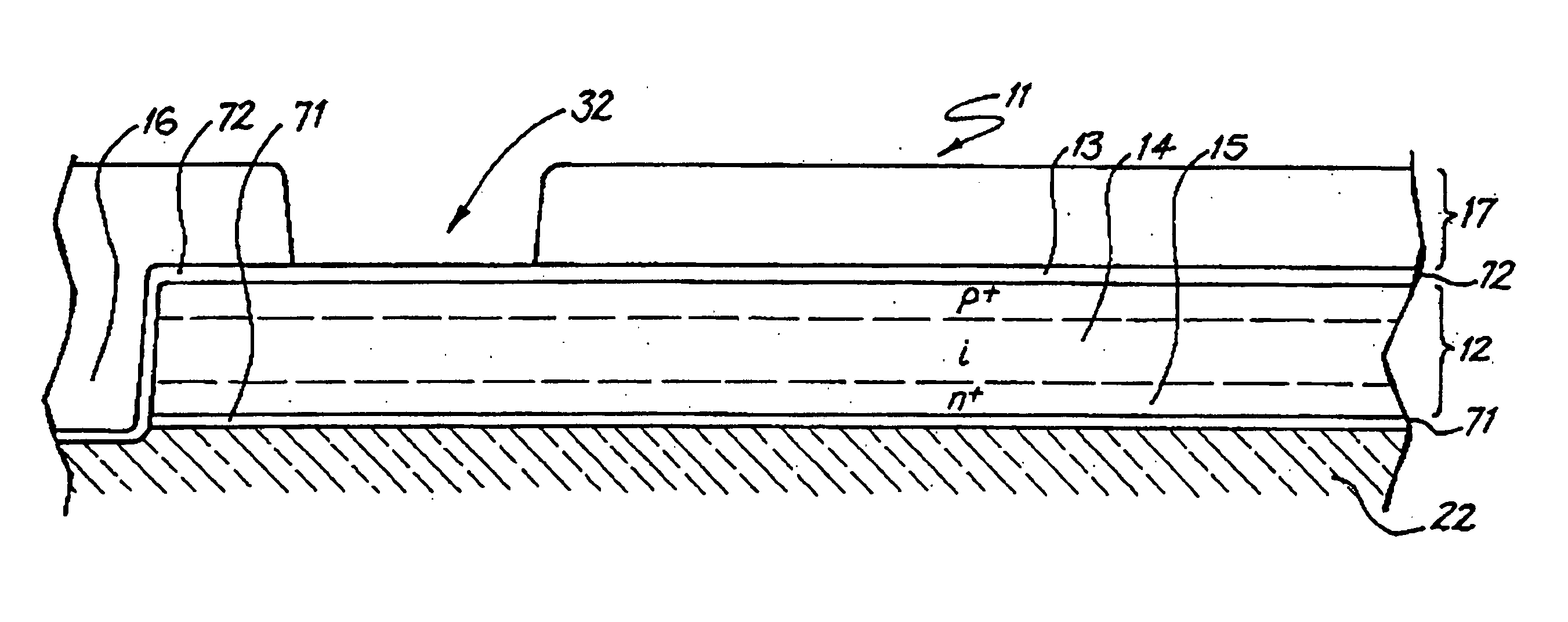
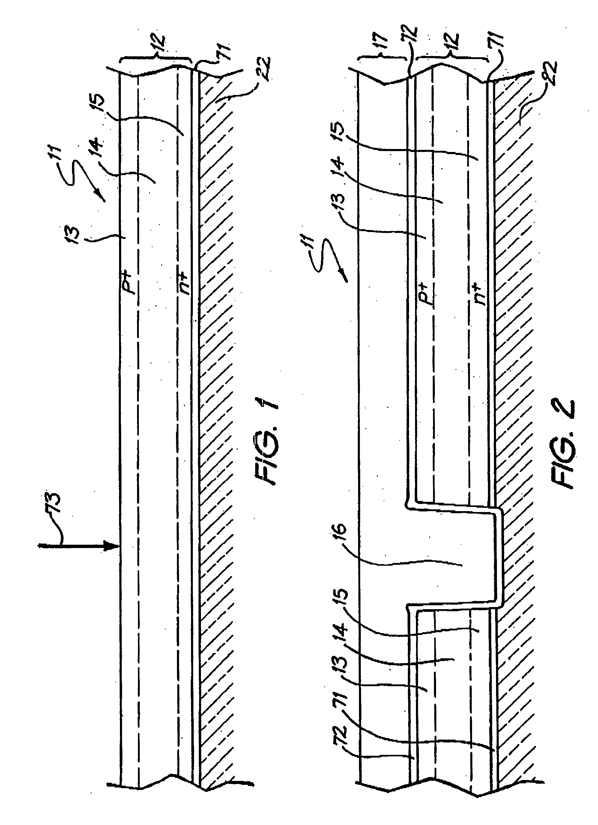
[0024] Referring to the drawings, FIG. 1 illustrates a part of a semiconductor structure 11 which is a precursor to the photovoltaic device fabrication process described below. The semiconductor structure 11 is formed as a thin semiconductor film applied to a substrate 22 in the form of a glass sheet to which a thin silicon nitride anti-reflection coating 71 has been applied. The anti-reflection coating 71 has a thickness of 80 nm. For optimal performance, the thin semiconductor film comprises a thin polycrystalline silicon film 12 formed with a total thickness in the range of 1 to 2 μm and preferably 1.6 μm. The polycrystalline silicon film 12 has an upper p+ type region 13 which is 60 nm thick, a lower n+ type region 15 which is 40 nm thick, and a 1.5 μm thick intrinsic or lightly p type doped region 14 separating the p+ and n+ type regions. The sheet resistance in both n+ type and p+ type layers is preferably between 400 and 2500Ω / □, with no more than 2×1014 cm−2 boron in total. ...


PUM

PropertyMeasurementUnit
Viscosityaaaaaaaaaa
Fractionaaaaaaaaaa
Viscosityaaaaaaaaaa

Abstract

Silicon (12) is etched through a mask (11) comprising a layer of organic resin material (such as novolac) through which openings (32) are formed in the areas to be etched. The layer of organic resin is first deposited over a free surface of the device to be etched. The openings (32) are then formed by depositing droplets of a caustic etchant such as sodium hydroxide (NaOH) or potassium hydroxide (KOH) with an inkjet printer. The etchant reacts with the resin to expose the silicon surface in areas to be etched. The etching of the silicon surface is performed by applying a dilute solution of hydrofluoric acid (HF) and potassium permanganate (KMnO4) to the exposed surface through the openings in the mask to etch the silicon to a desired depth (83).

Description

FIELD OF THE INVENTION [0001] The present invention relates generally to the field of semiconductor device fabrication and in particular the in invention provides an improved processing step for use in a method of forming metal contacts and other structures in thin film semiconductor devices. A new device structure for thin film photovoltaic devices is also provided. BACKGROUND OF THE INVENTION [0002] A major advantage of thin-film photovoltaic (PV) modules over conventional wafer-based modules is the potential for low cost of production. However in practice cost savings have been difficult to achieve as a major component of cost is the number and complexity of process steps involved in the manufacturing sequence and can quickly outweigh savings in material costs. In particular the number of steps that require precise alignment, or the speed of the equipment used to perform a step can have a strong bearing on cost, as can the robustness of a process, which might in some cases lead t...

Claims


Application Information

Patent Timeline
IPC IPC(8): H01L21/76H01L21/308H01L21/3213H01L21/467H01L27/142H01L31/18
CPCH01L21/32134H01L21/32139H01L31/046Y02E10/547H01L31/1804Y02P70/50
Inventor YOUNG, TREVOR LINDSAY
Owner CSG SOLAR AG
Why Eureka
Try Eureka