
Minute structure, micromachine, organic transistor, electric appliance, and manufacturing method thereof

a micromachine and organic transistor technology, applied in microstructural technology, microstructural devices, thermoelectric devices, etc., to achieve the effect of large-scale integrated devices and low cos

Active Publication Date: 2007-01-04
SEMICON ENERGY LAB CO LTD
View PDF33 Cites 42 Cited by
  • Summary
  • Abstract
  • Description
  • Claims
  • Application Information

AI Technical Summary

Benefits of technology

The present invention provides a minute structure with a frame-shaped frame and high light transmittance. The minute structure can be integrated into a display portion, allowing for a high aperture ratio. The invention also includes various examples of the minute structure, including a first layer and a second layer formed over an insulating surface, a space formed inside the frame below the second layer, and an organic semiconductor layer formed inside the space. The invention also provides an organic transistor with the minute structure and an electric appliance comprising the organic transistor. The technical effects of the invention include improved display quality and higher aperture ratio.

Problems solved by technology

However, a description of a semiconductor device to control a micromachine is not made, and of course there is no description of a device in which a semiconductor device is formed integrally.

Method used


Image

  • Minute structure, micromachine, organic transistor, electric appliance, and manufacturing method thereof
  • Minute structure, micromachine, organic transistor, electric appliance, and manufacturing method thereof
  • Minute structure, micromachine, organic transistor, electric appliance, and manufacturing method thereof

Examples


embodiment mode 1

[0047] In this embodiment mode, a structure of a minute structure is described.

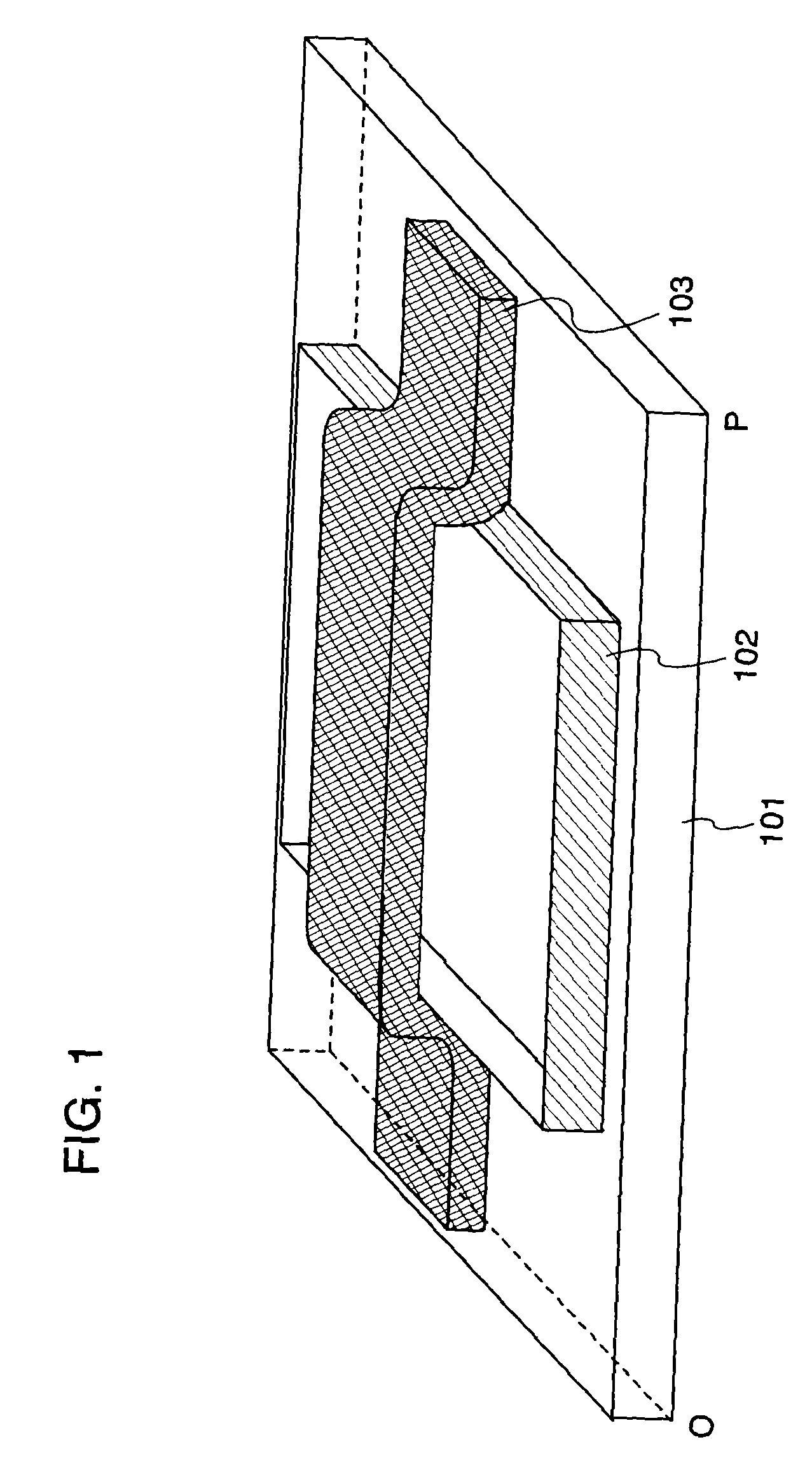
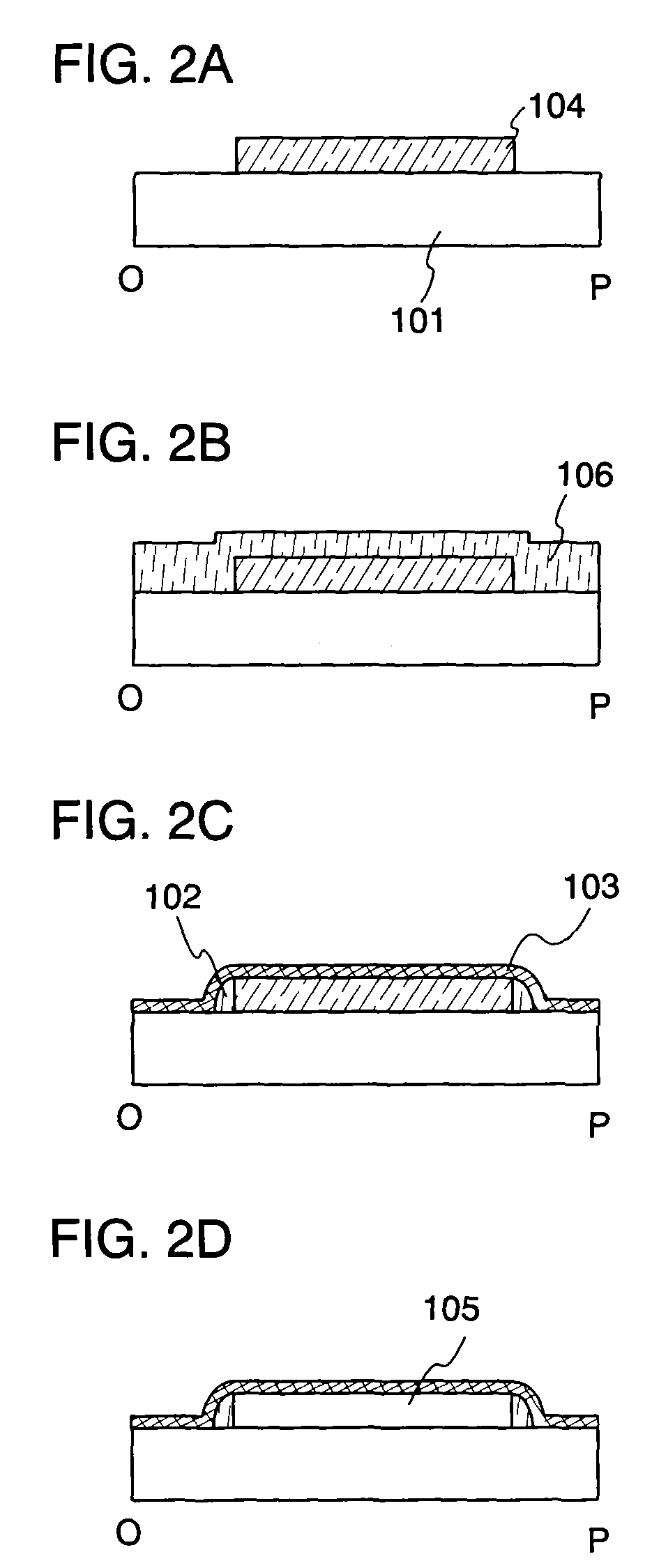
[0048] As shown in FIG. 1, a minute structure of the present invention has a first layer 102 having a frame-shape over an insulating surface 101. In other words, the frame formed of the first layer 102 is two pairs of walls. Note that a space 105 needs to be provided below the second layer 103; therefore, a frame supporting the second layer 103 may have at least two sides. That is, at least one pair of walls is formed.

[0049] The space is provided inside the frame formed of the first layer 102. In other words, a space is provided so as to be surrounded by the frame. The insulating surface is a surface of a glass substrate, a quartz substrate, a plastic substrate, or the like. By forming a minute structure over a plastic substrate, a device with high flexibility and a thin thickness can be formed. In addition, a glass substrate which is thinned by polishing may be used. By polishing, a thin device can be ...

embodiment mode 2

[0067] In this embodiment mode, a structure of a measurement element using a minute structure is described.

[0068] As shown in FIG. 3, in a minute structure as described above, a conductor (hereinafter, referred to as a lower electrode since it serves as a lower electrode) 110 is formed below a sacrifice layer and patterned into a predetermined shape. The lower electrode 110 can be formed of a metal material such as titanium (Ti), aluminum (Al), molybdenum (Mo), and tungsten (W); or a compound of the metal material (such as metal oxide and metal nitride). An element such as neodymium (Nd) and scandium (Sc) are preferably added to a material with low heat resistance such as aluminum (Al) so as to avoid a hillock due to heating. Note that neodymium is favorable to be used as a material to be added since resistance of aluminum is not heightened due to neodymium rather than scandium.

[0069] Then, the sacrifice layer is formed over the lower electrode 110 and patterned into a predetermin...

embodiment mode 3

[0077] In this embodiment mode, a structure of an element which is different from that of the foregoing embodiment modes is described.

[0078] In a minute structure shown in FIG. 1, the second layer 103 can be used as a filament and the minute structure of the present invention can be applied to a protective circuit. When excessive voltage is applied to the second layer 103, the second layer 103 is cut; therefore, the minute structure can be used as a protective circuit. In the case where the second layer 103 is not to be cut, if a physical property of the second layer 103 changes due to current applied to the second layer 103, the minute structure can be used as a protective circuit by utilizing the change in a property.

[0079] When the minute structure is used as a protective circuit, the second layer 103 is preferably formed with a conductor.


PUM


Abstract

A micromachine is generally formed using a semiconductor substrate such as a silicon wafer. One of the objects of the present invention is to realize further reduction in cost by integrating a minute structure and a semiconductor element controlling the minute structure over one insulating surface in one step. A minute structure has a structure in which a first layer formed into a frame-shape are provided over an insulating surface, a space is formed inside the frame, and a second layer is formed to cross over the first layer. Such a minute structure and a thin film transistor can be integrated over one insulating surface in one step.

Description

BACKGROUND OF THE INVENTION [0001] 1. Field of the Invention [0002] The present invention relates to a minute structure, a micromachine having the minute structure, an organic transistor having the minute structure and an electric appliance having the organic transistor. In addition, the present invention relates to a manufacturing method thereof. [0003] 2. Description of the Related Art [0004] In recent years, a micro mechanical system called MEMS is actively researched. MEMS is an abbreviated name of a micro electro mechanical system, which is sometimes simply called a micromachine. A micromachine in general corresponds to a minute device in which “a movable micro structure having a three-dimensional structure” and “an electric circuit having a semiconductor element” are integrated. Unlike a semiconductor element, the foregoing micro structure has a three-dimensional structure and a movable portion. [0005] In addition, a technique for forming each kind of device, which is a microm...

Claims


Application Information

Patent Timeline
Patent Type & Authority Applications(United States)
IPC IPC(8): H01L27/12H01L21/84H10K99/00
CPCH01L51/0021H01L27/1214H01L27/1255H01L27/1266H10K71/60B81B3/00B81C1/00
Inventor YAMAGUCHI, MAYUMIIZUMI, KONAMI
Owner SEMICON ENERGY LAB CO LTD
Learn More