Check patentability & draft patents in minutes with Patsnap Eureka AI!

METHOD OF ROOM TEMPERATURE GROWTH OF SIOx ON SILICIDE AS AN ETCH STOP LAYER FOR METAL CONTACT OPEN OF SEMICONDUCTOR DEVICES

a technology of semiconductor devices and etch stop layers, which is applied in the direction of individual semiconductor device testing, testing/measurement of semiconductor/solid-state devices, electrical apparatus, etc., can solve the problems of weak driving current or contact resistance problems, etch surface damage, contact resistance problems

Inactive Publication Date: 2007-01-11
IBM CORP
View PDF17 Cites 8 Cited by
  • Summary
  • Abstract
  • Description
  • Claims
  • Application Information

AI Technical Summary

Benefits of technology

[0020] The present invention, providing an oxide film over the silicide, benefits from the fact that MC nitride RIE is more selective to oxide than silicide, therefore protecting the silicide.

Problems solved by technology

In 90 nm technology for silicon on insulator (SOI), because of thin Si, sometimes the MC RIE punches through the silicide and touches the surface of Si which causes weak driving current problems or contact resistance problems.
However, conventional SiOx deposition can cause the oxidation of silicide and it creates a resistance problem.
Although RIE leaves the etched surface damaged, it is a very common etching mode in semiconductor manufacturing.
This becomes a problem when the silicide 106 is thin and the Ti / TiN liner would then land on top of the silicon 104 instead of on the silicide 106, and this can cause a contact resistance problem.
However, the downside of such an approach would be Si consummption and contact resistance problems.
In bulk (non SOI) technology, the problem would be junction leakage.

Method used


Image

  • METHOD OF ROOM TEMPERATURE GROWTH OF SIOx ON SILICIDE AS AN ETCH STOP LAYER FOR METAL CONTACT OPEN OF SEMICONDUCTOR DEVICES
  • METHOD OF ROOM TEMPERATURE GROWTH OF SIOx ON SILICIDE AS AN ETCH STOP LAYER FOR METAL CONTACT OPEN OF SEMICONDUCTOR DEVICES
  • METHOD OF ROOM TEMPERATURE GROWTH OF SIOx ON SILICIDE AS AN ETCH STOP LAYER FOR METAL CONTACT OPEN OF SEMICONDUCTOR DEVICES

Examples


Embodiment Construction

[0034] In the description that follows, numerous details are set forth in order to provide a thorough understanding of the present invention. It will be appreciated by those skilled in the art that variations of these specific details are possible while still achieving the results of the present invention. Well-known processing steps are generally not described in detail in order to avoid unnecessarily obfuscating the description of the present invention.

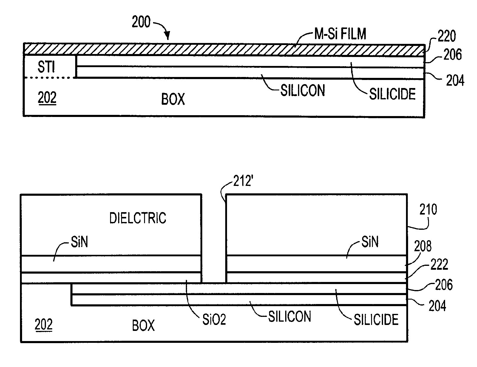
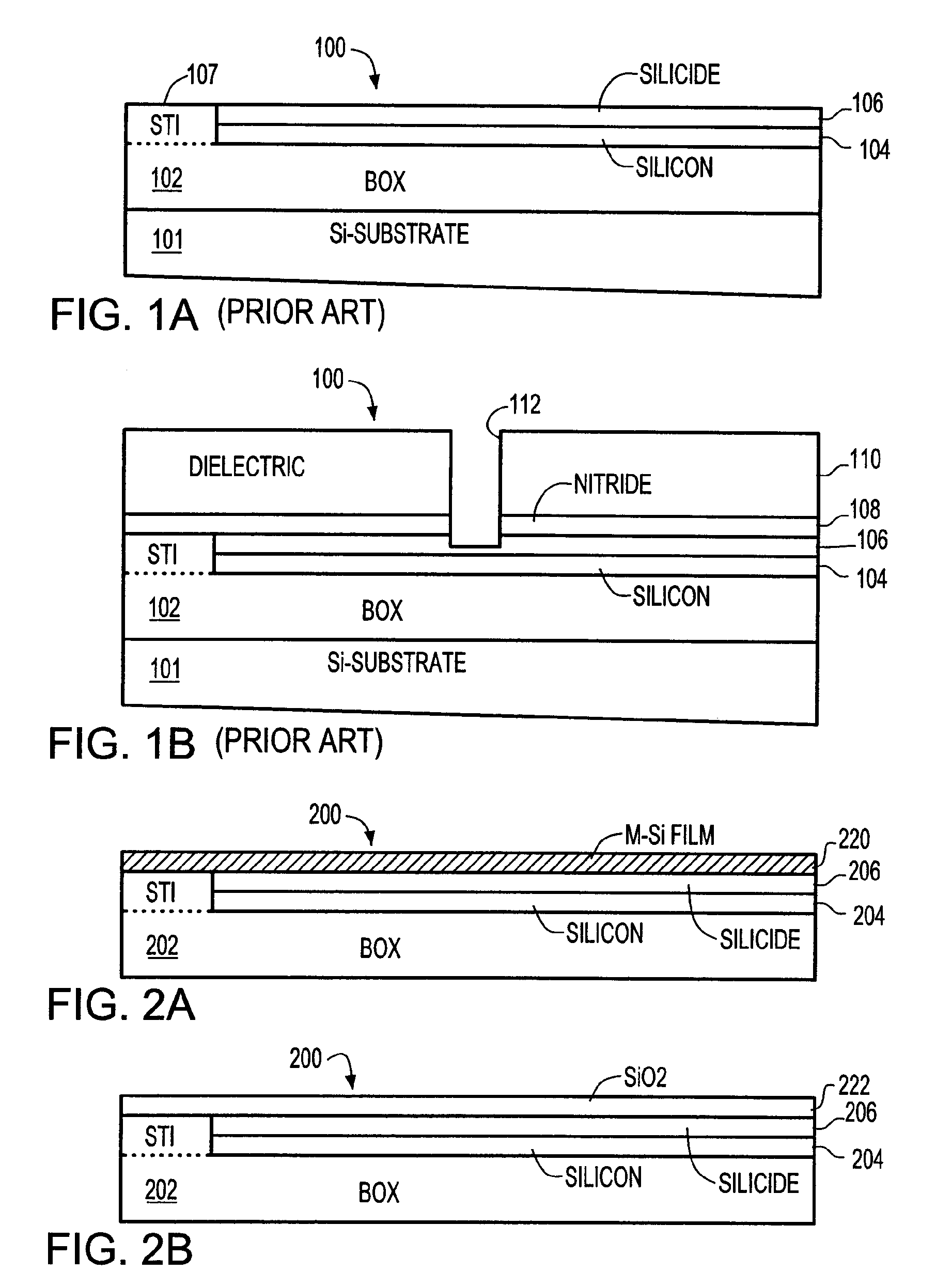
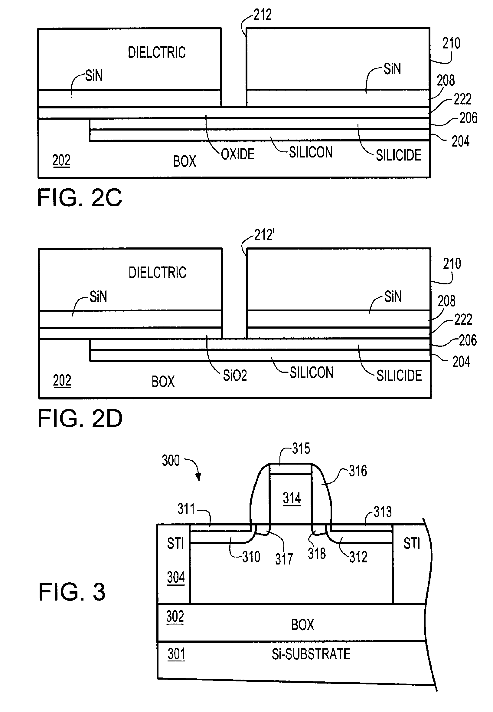
[0035] Materials (e.g., silicon dioxide) may be referred to by their formal and / or common names, as well as by their chemical formula. Regarding chemical formulas, numbers may be presented in normal font rather than as subscripts. For example, silicon dioxide may be referred to simply as “oxide”, chemical formula SiO2. For example, silicon nitride (stoichiometrically Si3N4, often abbreviated as “SiN”) may be referred to simply as “nitride”.

[0036] In the description that follows, exemplary dimensions may be presented for an illustr...


PUM


Abstract

Silicide is protected during MC RIE etch by first forming an oxide film over the silicide and, after performing MC RIE etch, etching the oxide film. The oxide film is formed from a film of alloyed metal-silicon (M-Si) on the layer of silicide, then wet etching the metal-silicon. An ozone plasma treatment process can be an option to densify the oxide film. The oxide film may be etched by oxide RIE or wet etch, using 500:1 DHF.

Description

BACKGROUND OF THE INVENTION [0001] The invention relates to semiconductor device fabrication techniques and, more particularly, to techniques for etching through a dielectric layer to an underlying silicide layer. [0002] Typically, source and drain regions in a modern MOSFET (Metal-Oxide-Semiconductor Field-Effect-Transistor) devices are formed with overlying silicide as the contact. Silicides are alloys of silicon and metals, and are used as contact materials in silicon device manufacturing. Exemplary silicides are cobalt silicide (CoSi2), nickel Silicide (NiSi), titanium silicide (TiSi2), tungsten silicide (WSi2), tantalum silicide (TaSi2), and platinum silicide (PtSi). [0003] Silicides are commonly used as conductors and contact materials in silicon semiconductor technology due to their high conductivity, compatibility with silicon, and suitability to small-geometry semiconductor devices. The high conductivity (low resistivity) of source / drain silicide serves to minimize the cont...

Claims


Application Information

Patent Timeline
IPC IPC(8): G01R31/26H01L21/44H01L21/66
CPCH01L21/28518H01L21/76897H01L21/76834
Inventor WANG, YUN-YULAVOIE, CHRISTIANMELLO, KEVIN E.MURRAY, CONAL E.OONK, MATTHEW W.
Owner IBM CORP
Features
  • R&D
  • Intellectual Property
  • Life Sciences
  • Materials
  • Tech Scout
  • Unparalleled Data Quality
  • Higher Quality Content
  • 60% Fewer Hallucinations
Learn More