

Semiconductor device and a manufacturing method of the same
a manufacturing method and semiconductor technology, applied in the direction of sustainable manufacturing/processing, final product manufacturing, printed circuit aspects, etc., can solve the problems of low mounting strength of lga and also the thickness of the packaging, so as to improve the mountability of the semiconductor device and the effect of the variation of the height of the solder coa
- Summary
- Abstract
- Description
- Claims
- Application Information
AI Technical Summary
Benefits of technology
Problems solved by technology
Method used
Image

Examples
embodiment
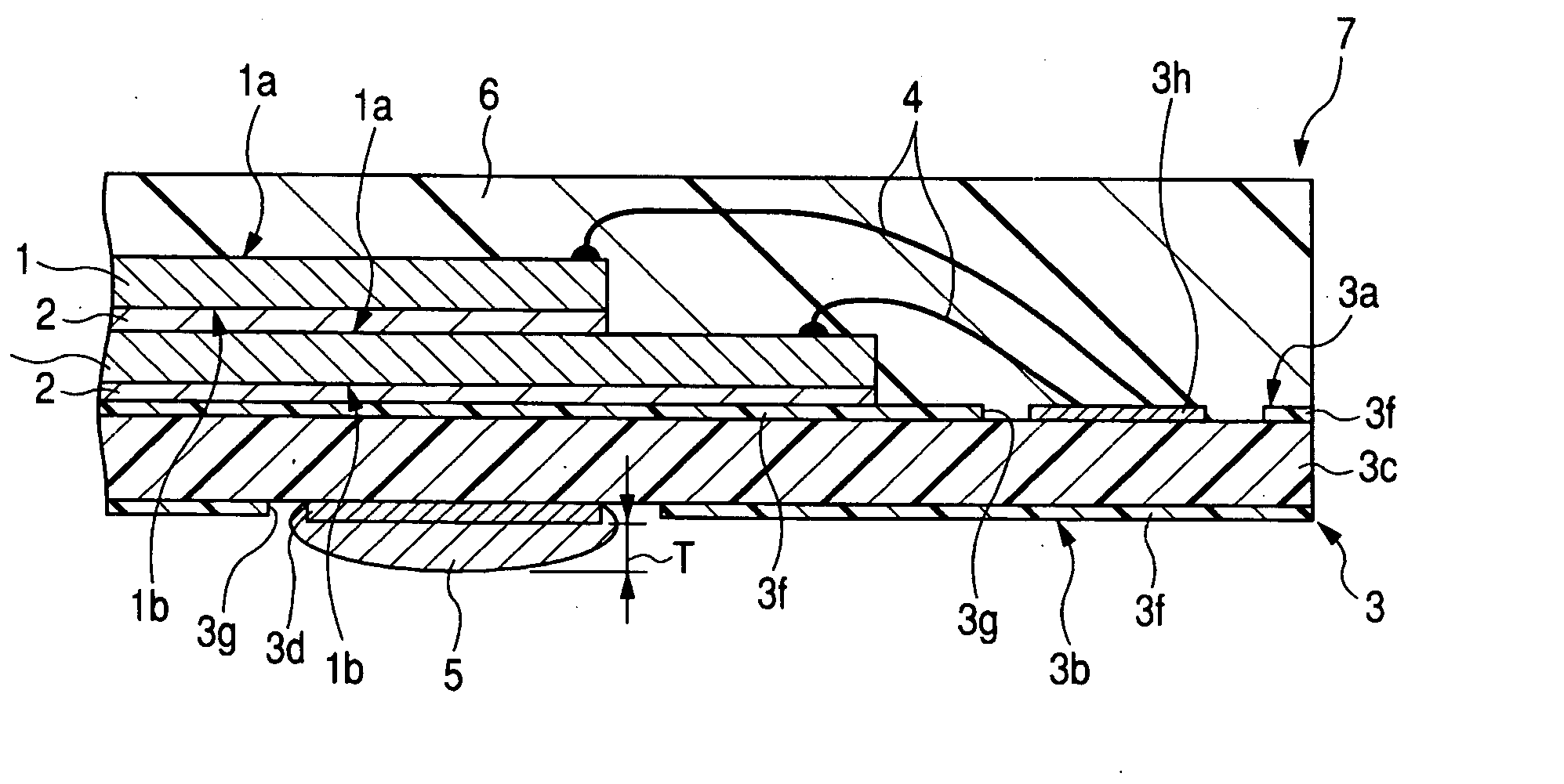
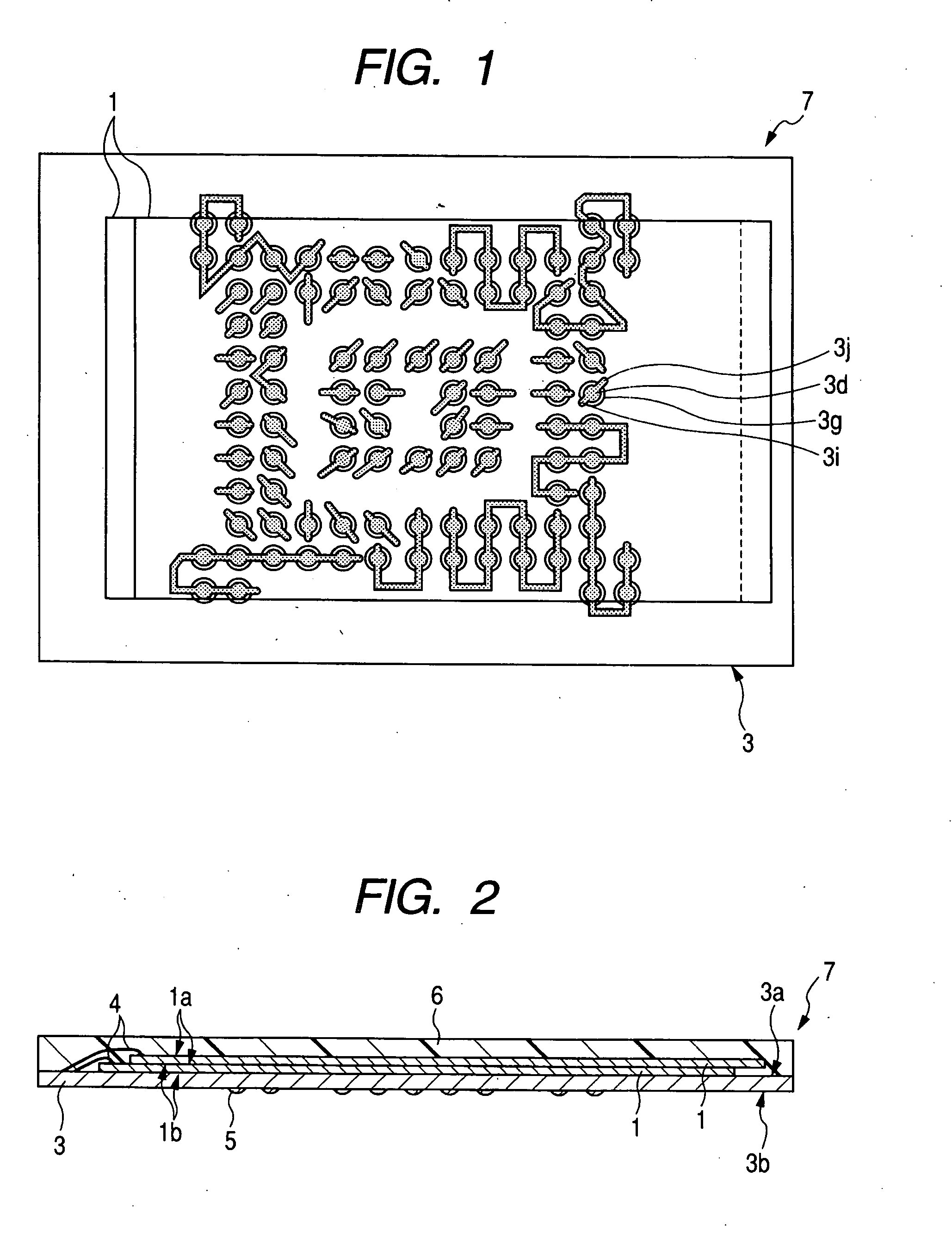
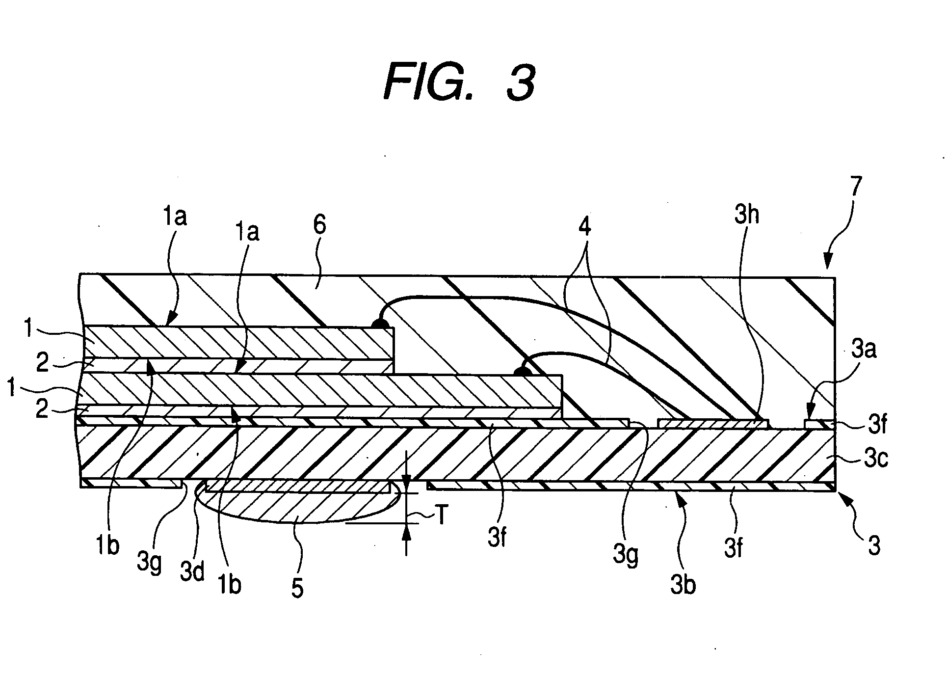
[0052]FIG. 1 is a plan view penetrating a sealing body and showing an example of the arrangement relation between a chip and a land in the structure of the semiconductor device of the Embodiment of the present invention, FIG. 2 is a cross-sectional view showing an example of the structure of the semiconductor device shown in FIG. 1, FIG. 3 is an enlarged partial sectional view showing an example of the structure of the semiconductor device shown in FIG. 2, FIG. 4 is a partial plan view showing an example of the structure of the land of the semiconductor device shown in FIG. 1, FIG. 5 is a cross-sectional view showing the structure cut along the A-A line of FIG. 4, FIG. 6 is a plan view penetrating a sealing body and showing the arrangement relation between a chip and a land in the structure of the semiconductor device of the modification of the Embodiment of the present invention, FIG. 7 is a cross-sectional view showing the structure of the semiconductor device of the modification ...
PUM
 Abstract
Description
Claims
Application Information