Portable microdisplay system

a micro-display and display technology, applied in the field of portable micro-display systems, can solve the problems of limiting the processing of further circuits to low temperatures, increasing the complexity of integrated circuits for displays, and limiting the material selection

Inactive Publication Date: 2007-01-25
ZAVRACKY MATTHEW +12
View PDF39 Cites 104 Cited by
  • Summary
  • Abstract
  • Description
  • Claims
  • Application Information

AI Technical Summary

Benefits of technology

[0020] One of the traits of liquid crystal that is desired is the long time constant which allows the image to be maintained without having to refresh in certain instances. While a long time constant is generally a benefit, it can be a detriment in instances where the display is powered down and powered up a short time later. Upon powering up the system, a portion of the previous image may remain.
[0021] In a preferred embodiment, an analog comparator samples the voltage of the main power in real time. When the voltage drops below the level to run the circuit plus some mar

Problems solved by technology

These materials are limited as they use silicon that is already on glass, which generally restricts further circuit processing to low

Method used


Image

  • Portable microdisplay system
  • Portable microdisplay system
  • Portable microdisplay system

Examples


Embodiment Construction

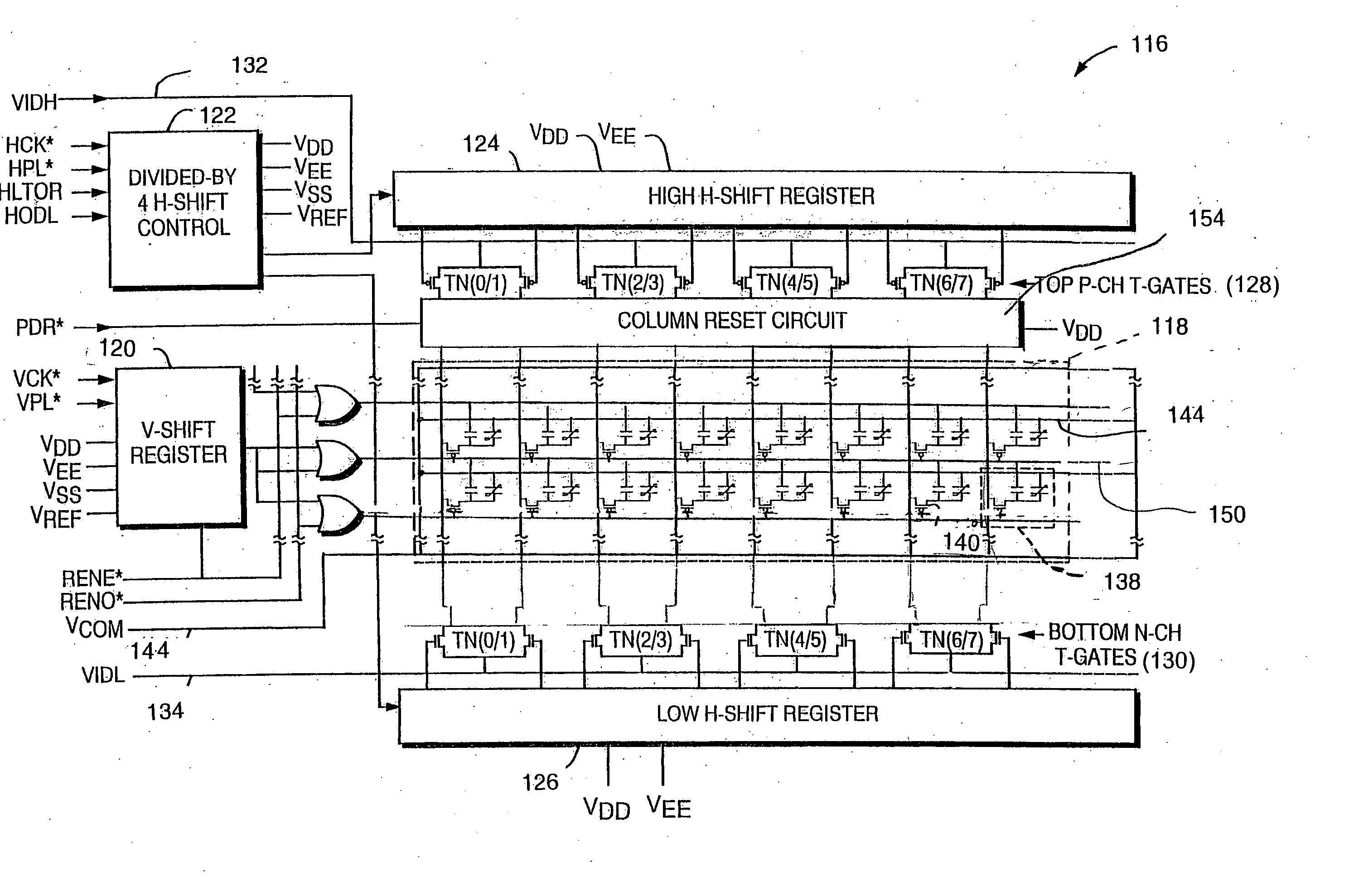
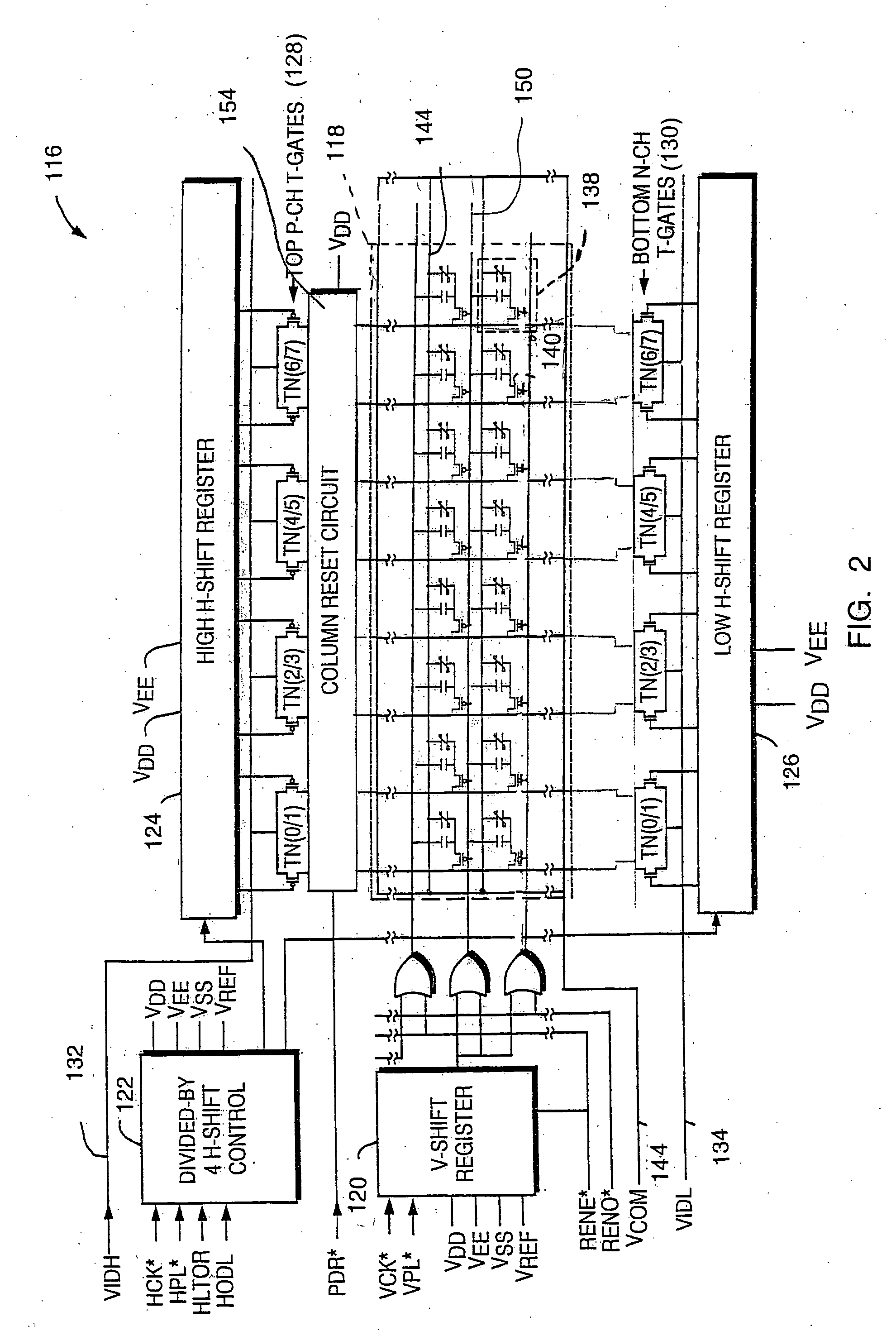
[0114] Referring to the drawings, where like numerals indicate like elements, there is illustrated a display in accordance with the present invention, generally referred to as 110 in FIG. 9, for example.

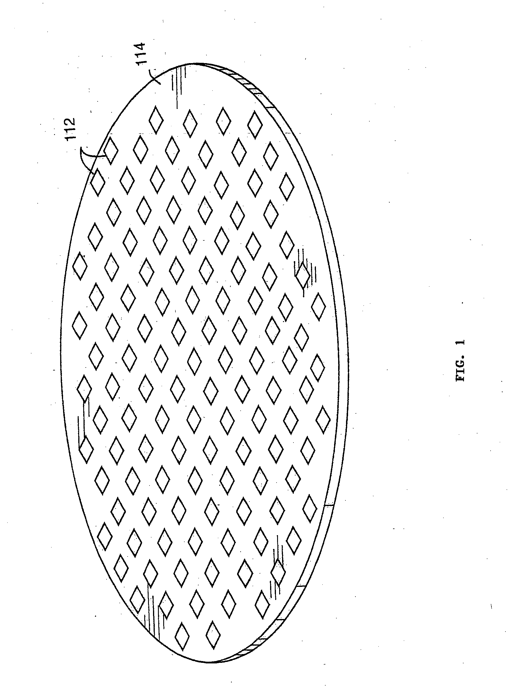
[0115] A preferred embodiment of the invention utilizes a process of making a plurality of flat panel displays 110 in which a large number of active matrix arrays 112 are fabricated on a single wafer 114 as illustrated in connection with FIG. 1.

[0116] The number of displays fabricated on a single wafer depends upon the size of the wafer and the size of each display. In a preferred embodiment, the wafer has a five inch diameter or larger. The size of each display depends on the resolution and pixel electrode size. In a display having a resolution of approximately 76,800 pixels (e.g. a 320×240 array), commonly referred to as QVGA, with a 0.24 inch diagonal display and the pixel electrodes having a width of 15 microns, the active display area is 4.8 mm×3.6 mm. The display die has dime...


PUM


Abstract

An active matrix color crystal display has an active matrix circuit, a counterelectrode panel and an interposed layer of liquid crystal. The active matrix display is located in a portable microdisplay system. The image is written to the the display therein causing the liquid crystal to move to a specific image position. A light source is flashed to illuminate the display. The pixel electrodes are set to a specific value to cause the liquid crystal to move towards a desired position. The process of writing, flashing, and setting the electrode intensity value to reorient the liquid crystal to produce an image is repeated. Portable system can include a digital camera, cellular telephone, camcorder, heads up display, instant print camera, pager,

Description

RELATED APPLICATIONS [0001] This application is a divisional application of U.S. application Ser. No. 09 / 460,960, filed on Dec. 14, 1999, which claims the benefit of U.S. application Ser. No. 60 / 112,147 filed on Dec. 14, 1998 and U.S. application Ser. No.60 / 121,899 filed on Feb. 26, 1999. The entire contents of all of these applications are incorporated herein by reference.BACKGROUND OF THE INVENTION [0002] Flat-panel displays are being developed which utilize liquid crystals or electroluminescent materials to produce high quality images. These displays are expected to supplant cathode ray tube (CRT) technology and provide a more highly defined television picture or computer monitor image. The most promising route to large scale high quality liquid crystal displays (LCDs), for example, is the active-matrix approach in which thin-film transistors (TFTs) are co-located with LCD pixels. The primary advantage of the active matrix approach using TFTs is the elimination of cross-talk betw...

Claims


Application Information

Patent Timeline
IPC IPC(8): G09G3/36G02F1/1335G02F1/133G02F1/13357G09F9/30G09F9/35G09G3/20G09G3/34G09G5/00G09G5/399H04N5/225H04N5/765H04N5/907
CPCG09G3/3406G09G2360/144G09G3/3614G09G3/3648G09G3/3655G09G3/3659G09G3/3677G09G3/3688G09G5/008G09G5/399G09G2300/0876G09G2310/0235G09G2310/0237G09G2310/024G09G2310/0251G09G2310/0281G09G2310/0291G09G2310/0297G09G2310/08G09G2320/02G09G2320/0247G09G2320/0276G09G2320/041G09G2320/0606G09G2320/0626G09G2320/0633G09G2320/0666G09G2340/0414G09G2340/0421G09G3/3413G09G3/36
Inventor ZAVRACKY, MATTHEWHERRMANN, FREDERICK P.CHERN, WEN-FOORICHARD, ALANGALE, RONALD P.LO, JASONELLERTSON, DAVIDTSAI, KUOJINNGFAN, JOHN C.C.TSAUR, BOR-YEUPOMBO, STEPHEN A.BUMGARDNER, RODNEYVU, DUY-PHACH
Owner ZAVRACKY MATTHEW
Why Eureka
Try Eureka