Organic photoconductor, process cartridge and image forming apparatus both employing the same

a photoconductor and process cartridge technology, applied in the direction of electrographic process apparatus, instruments, corona discharge, etc., can solve the problems of deterioration of the photoconductor, adverse effects on the human body, etc., and achieve excellent sharpness and stability

Inactive Publication Date: 2007-01-25
KONICA MINOLTA BUSINESS TECH INC
View PDF10 Cites 8 Cited by
  • Summary
  • Abstract
  • Description
  • Claims
  • Application Information

AI Technical Summary

Benefits of technology

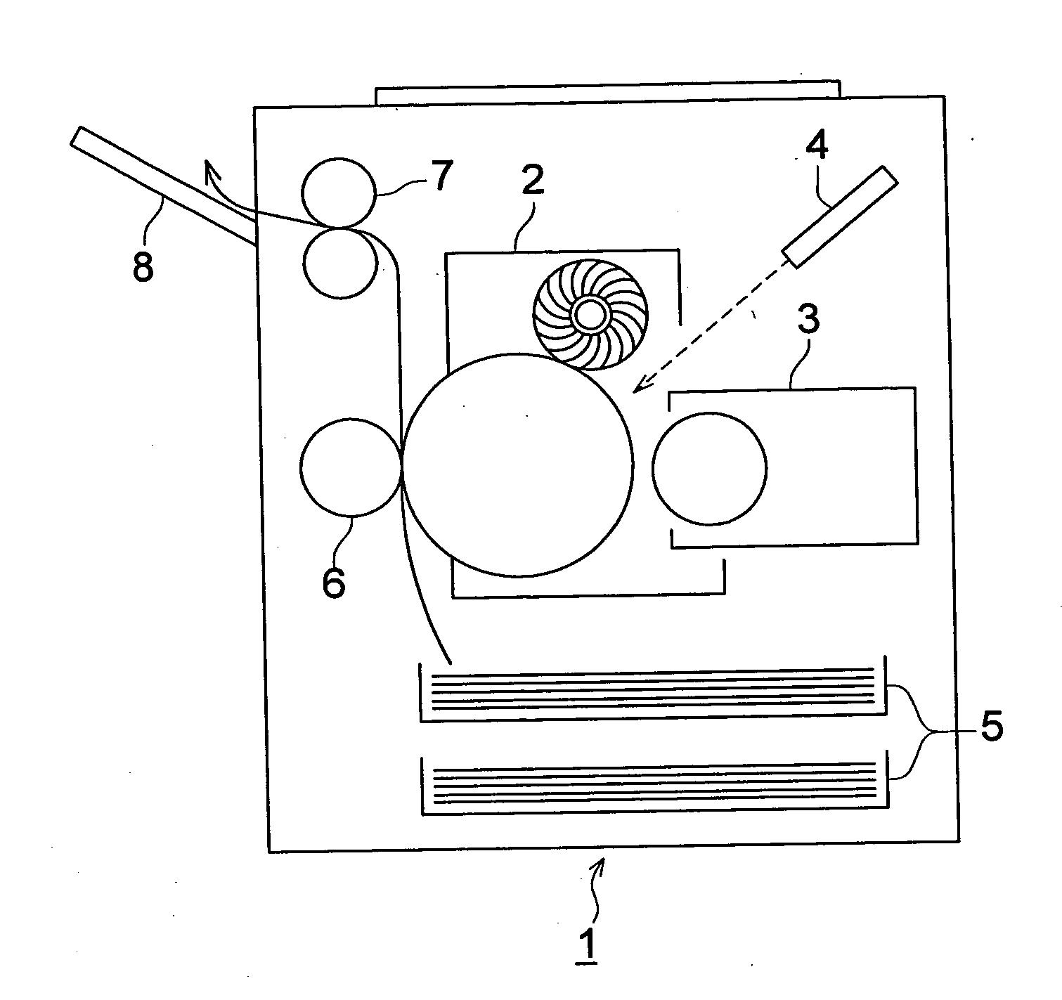
[0017] An object of the invention is to solve the aforementioned problems of the organic photoconductor used in an image forming apparatus of a contact charging type, and in particular, to solve the aforesaid problems of the organic photoconductor having the surface layer containing fluorine-containing resin particles and to prevent generation of image defects such as dielectric breakdown, black spots or dash marks and thereby to provide an organic photoconductor, a process cartridge and an image forming apparatus which can form images having excellent sharpness and stability for a long time.

Problems solved by technology

However, the corona discharger needs to be applied with high voltage, and therefore, an amount of generation of ionized oxygen, ozone, moisture and nitrogen oxide is large, resulting in problems that the organic photoconductor (hereinafter referred to also as photoconductor) is deteriorated, and the human body is adversely affected.
However, in contact charging method with a charging roller, if a support of organic photoconductor processed to prevent interference fringes (hereinafter referred to as moiré) caused by laser beam exposure is used, namely, if an aluminum support whose surface is roughened by cutting is used, there is caused a problem that dielectric breakdown is easily caused by convex portions on the surface subjected to cutting.
Further, if the surface of the organic photoconductor is charged repeatedly, cracks and contamination are generated on the organic photoconductor, resulting in various troubles that electric charges are concentrated on a portion of cracks and contamination, image defects such as dielectric breakdown and black spots are easily generated, and blurred images tend to be caused.
In particular, these problems tend to occur under the conditions of high temperature and high humidity, and low temperature and low humidity.
In addition, the organic photoconductor has a problem that its surface tends to be worn away because of friction against the contact charging member or a cleaning member.
However, if abrasion resistance of the organic photoconductor is improved by using the binder stated above, inorganic external additives such as silica in a developer is embedded in the surface of the organic photoconductor by pressure of the contact charging member, thus, the surface of the organic photoconductor tends to be contaminated by components of the external additives, and dash mark (small streak images in a form of a comet) and dielectric breakdown are easily caused, although abrasion resistance is improved.
However, in the organic photoconductor having in its surface the particles of fluorine-containing resin which has been reported so far, a fluorine-containing resin particle is easily separated from the binder on a boundary between them in the surface layer, thus, electric charges of the contact charging means tend to flow in the boundary surface, and dielectric breakdown and black spots are easily generated.
Further, external additives of toner concerning the contact charging means easily adhere to the boundary surface between the fluorine-containing resin particle and the binder, and blurred images and dash mark (small streak images in a form of a comet) are generated, which easily deteriorates sharpness of text images and halftone images.
However, in the fluorine-containing resin particles having low crystallinity, fluorine-containing resin particles tend to adhere to each other, dispersion stability in coating dispersion is low, the particles tend to cohere each other to form a coarse aggregated particle, resulting in problems that a surface layer having uniform characteristics is hardly formed, dash marks and blurred images are generated and halftone images are roughened.

Method used


Image

  • Organic photoconductor, process cartridge and image forming apparatus both employing the same
  • Organic photoconductor, process cartridge and image forming apparatus both employing the same
  • Organic photoconductor, process cartridge and image forming apparatus both employing the same

Examples


examples

[0195] Although examples are given and this invention is hereafter explained to details, the aspect of this invention is not limited to this. Incidentally, “part” in the following sentences represents “parts by mass”.

Manufacture of Photoconductor 1-1

[0196] The cylinder type aluminum base support, which surface has 10 points surface roughness Rz of 0.81 μm measured according to regulation of JISB-0601 by subjecting to cutting process and washed, was subjected to coating with the following interlayer coating composition by dipping and thereafter drying at 120 c. degree for 30 minutes, an interlayer having dry thickness of 1.0 μm was prepared.

[0197] The following intermediate layer dispersion liquid was diluted twice with the same mixed solvent, and filtered after settling for overnight (filter; Nihon Pall Ltd. company make RIGIMESH 5 μm filter, pressure at 50 kPa), whereby the intermediate layer coating solution was produced.

(Preparation of intermediate layer dispersion)Binder re...


PUM

PropertyMeasurementUnit
contact angleaaaaaaaaaa
number average primary particle sizeaaaaaaaaaa

Abstract

An image forming apparatus has an organic photoconductor having a surface layer containing fluorine-containing resin particles whose number average primary particle size is not less than 0.02 μm and is less than 0.20 μm; a charging device to charge by bring an charging member in contact with the organic photoconductor; a latent image forming device to for a latent image on the organic photoconductor; a developing device to visualize the latent image with toner and to form a toner image on the organic photoconductor; and a transferring device to transfer the toner onto a transfer material.

Description

BACKGROUND OF THE INVENTION [0001] The present invention relates to an organic photoconductor used in the field of a copying machine and a printer, a process cartridge and an image forming apparatus both employing the organic photoconductor. [0002] Compared with an inorganic photoconductor such as a selenium-based photoconductor and an amorphous silicone photoconductor, an organic photoconductor has great advantages including a broad range of selection for materials, an excellent aptitude for environment and low manufacturing cost, and the organic photoconductor has recently become a leading electrophotographic photoconductor, replacing an inorganic photoconductor. [0003] In an image forming method based on Carlson method, on the other hand, an organic photoconductor is charged electrically, then, an electrostatic latent image is formed thereon, then, a toner image is formed therefrom, and the toner image is transferred onto a transfer sheet to be fixed thereon to become a final ima...

Claims


Application Information

Patent Timeline
Patent Type & Authority Applications(United States)
IPC IPC(8): G03G21/18G03G15/02
CPCG03G5/0539G03G5/0592G03G5/0596G03G2215/00957G03G5/14791G03G5/14795G03G5/14726
Inventor INAGAKI, KEIICHITOKUTAKE, SHIGEAKI
Owner KONICA MINOLTA BUSINESS TECH INC
Why Eureka
Try Eureka