System and method for semiconductor processing

Active Publication Date: 2007-01-25
ASM INTERNATIONAL
View PDF10 Cites 3 Cited by
  • Summary
  • Abstract
  • Description
  • Claims
  • Application Information

AI Technical Summary

Benefits of technology

[0014] Advantages of the system may include one or more of the following. The system can instantaneously deliver a significant amount of energy to the wafer surface to initiate a desirable surface reaction. The system can perform a combination of pulsed plasma and/or flash heating to thermally activate chemical precursors on the surface of the substrate at temperatures slightly below that required to initiate a sustained thermal reaction. This technique can be used to build extremely thin layers of material for Atomic Layer Deposition processes. The system offers better control thickness. Customer can use thinner films to achieve the same result, thereby extending Moore's law. The resulting high quality films possess superior properties such as high uniformity, controlled resistivity, high diffusion resistance, and high conformality, among others. Thus, the system enables high precision etching, deposition or sputtering performance. The pulse modulation of a flash bulb and/or a radio frequency powered plasma source enables a tight control the radical production ratio in plasmas, the ion temperature and the charge accumulation. Also, since the time for accumulation of charges in a wafer is on the order of milli-seconds and the accumulation of charges to the w

Problems solved by technology

The load match is usually a motorized automatic tuner, so the load match operation incurs a predetermined time delay before the system is properly configured.
As noted in U.S. Pat. No. 5,468,341 entitled “Plasma-etching Method and Apparatus Therefor,” the amount of ion energy reaching a surface of the object to be etched in conventional RF sources can be accomplished by controlling the power of RF waves, the controllable range of dissociation process in plasmas is narrow, and, therefore, the extent of controllable etching rea

Method used


Image

  • System and method for semiconductor processing
  • System and method for semiconductor processing
  • System and method for semiconductor processing

Examples


Example

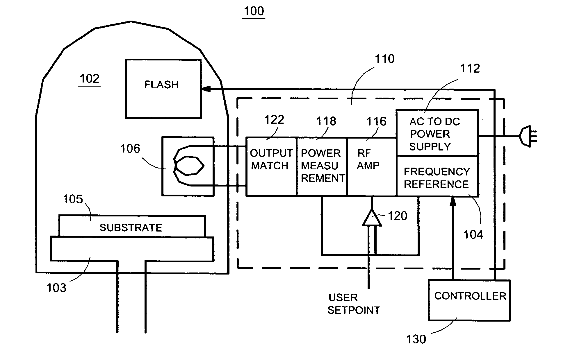
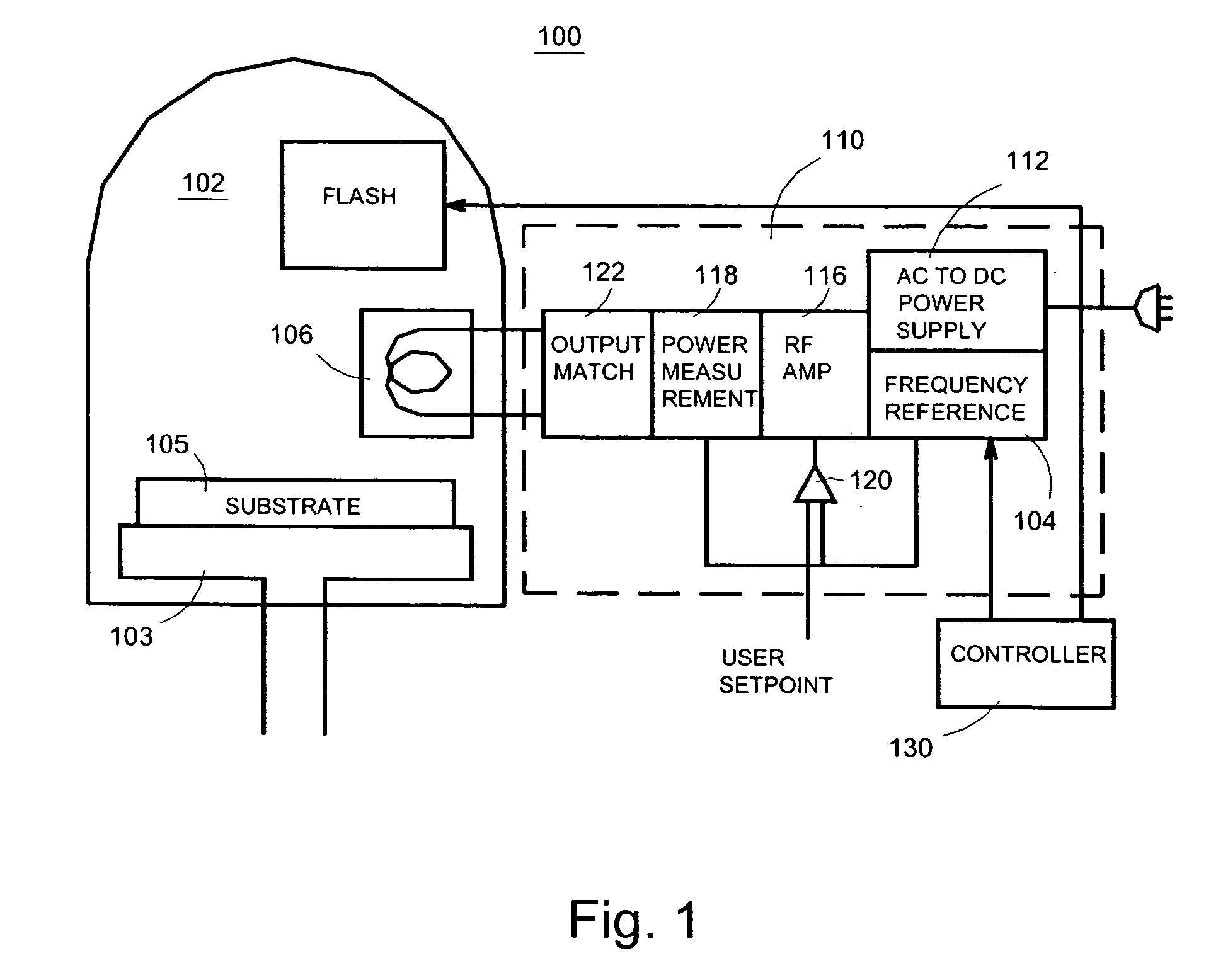
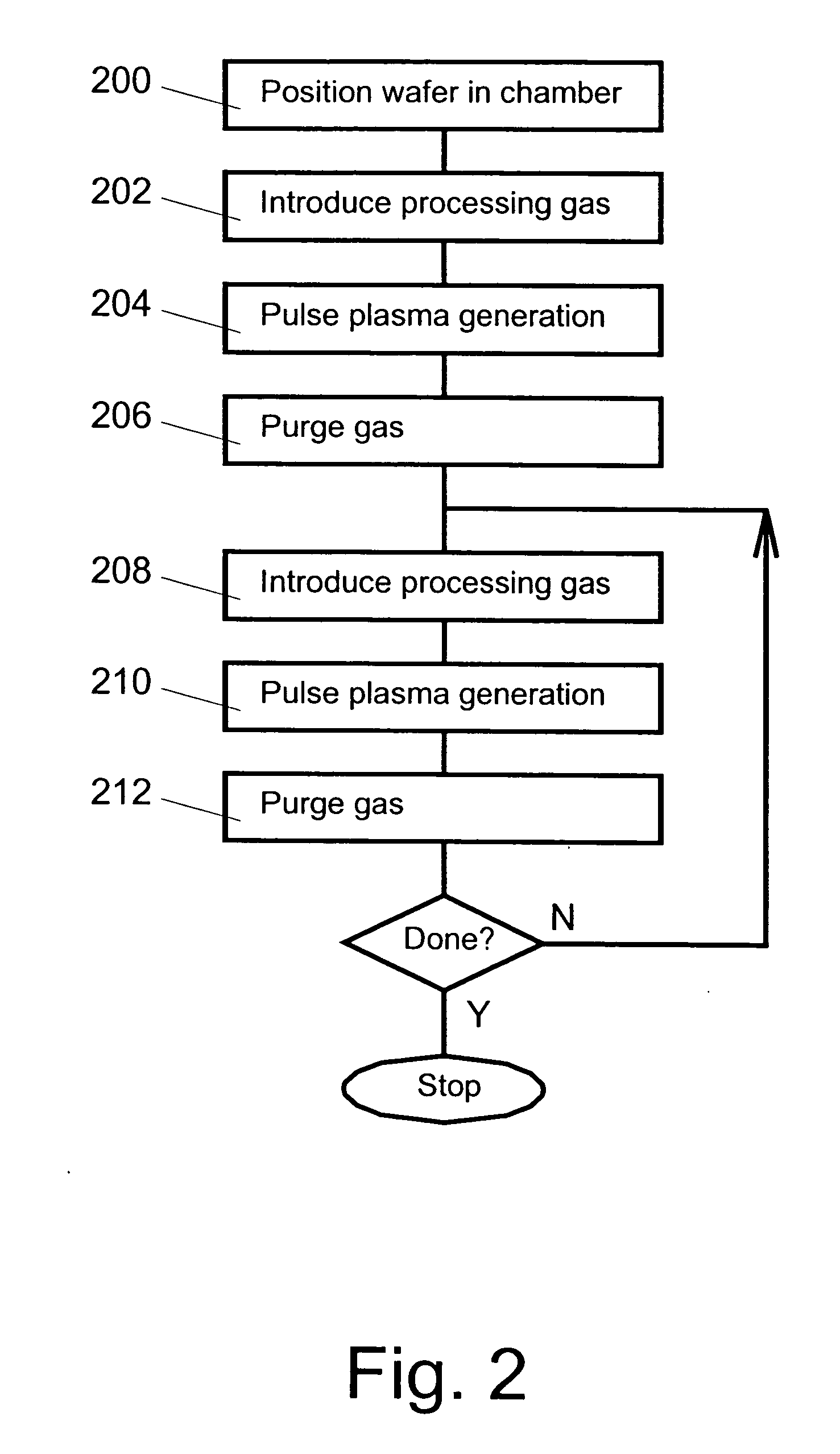
[0022]FIG. 1 shows an exemplary pulsed processing system 100 with a processing chamber 102. The processing chamber 102 has a chamber body enclosing components of the processing chamber such as a chuck 103 supporting a substrate 105. The processing chamber typically maintains vacuum and provides a sealed environment for process gases during substrate processing. On occasions, the process chamber needs to be periodically accessed to cleanse the chamber and to remove unwanted materials cumulating in the chamber. To support maintenance for the process chamber, an opening is typically provided at the top of the process chamber that is sufficiently large to provide access to the internal components of the process chamber.

[0023] The chamber 102 includes a plasma excitation circuit 106 driven by a solid-state plasma generator 110 with fast ignition capability. One commercially available plasma source is the Litmas source, available from LITMAS Worldwide of Matthews, N.C. The generator 110 ...


PUM


Abstract

Systems and methods are disclosed to perform semiconductor processing with a process chamber; a flash lamp adapted to be repetitively triggered; and a controller coupled to the control input of the flash lamp to trigger the flash lamp. The system can deploy a solid state plasma source in parallel with the flash lamp in wafer processing.

Description

CLAIM OF PRIORITY [0001] This application is a continuation-in-part application of U.S. patent application Ser. No. 10 / 403,211, filed Apr. 1, 2003, which is a divisional application of U.S. patent application Ser. No. 09 / 840,349, filed Apr. 21, 2001, now U.S. Pat. No. 6,610,169. CROSS-REFERENCE TO RELATED APPLICATION [0002] This application is related to U.S. patent application Ser. No. 11 / ______, filed ______, 2006, and entitled SEMICONDUCTOR PROCESSING SYSTEM AND METHOD. This application is incorporated herein in its entirety.BACKGROUND OF INVENTION [0003] The present invention relates to semiconductor processing. [0004] The fabrication of modern semiconductor device structures has traditionally relied on plasma processing in a variety of operations such as etching, depositing or sputtering. Plasma etching involves using chemically active atoms or energetic ions to remove material from a substrate. Plasma Enhanced Chemical Vapor Deposition (PECVD) uses plasma to dissociate and act...

Claims


Application Information

Patent Timeline
IPC IPC(8): H01L21/28
CPCH01J37/32009H01L21/67248H01L21/67115H01J37/32339
Inventor NGUYEN, TUENGUYEN, TAI DUNGBERCAW, CRAIG ALAN
Owner ASM INTERNATIONAL
Why Eureka
Try Eureka