Method of operating non-volatile memory device
- Summary
- Abstract
- Description
- Claims
- Application Information
AI Technical Summary
Benefits of technology
Problems solved by technology
Method used
Image

Examples
Embodiment Construction
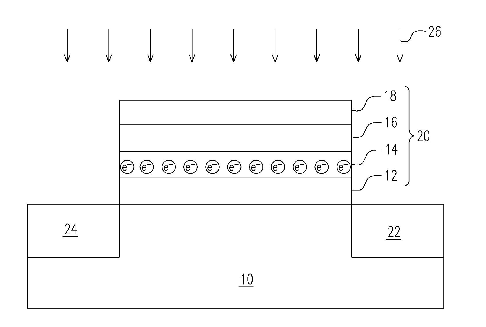
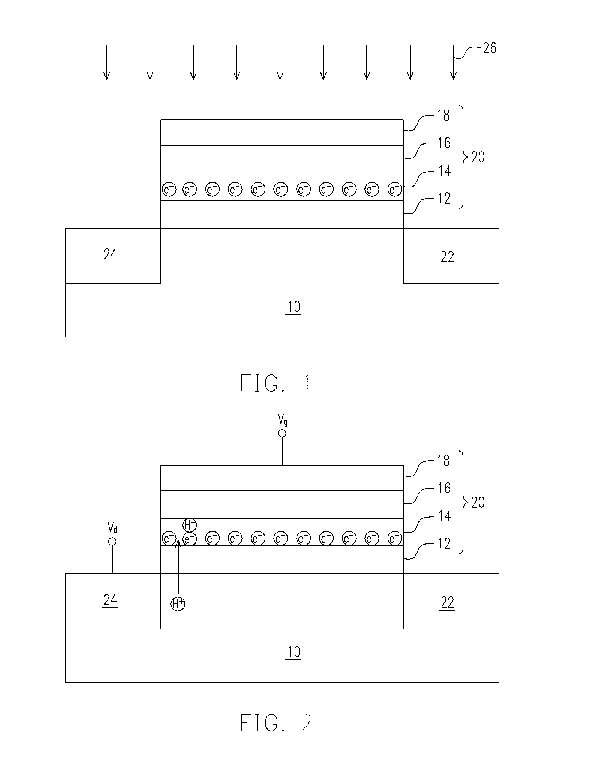
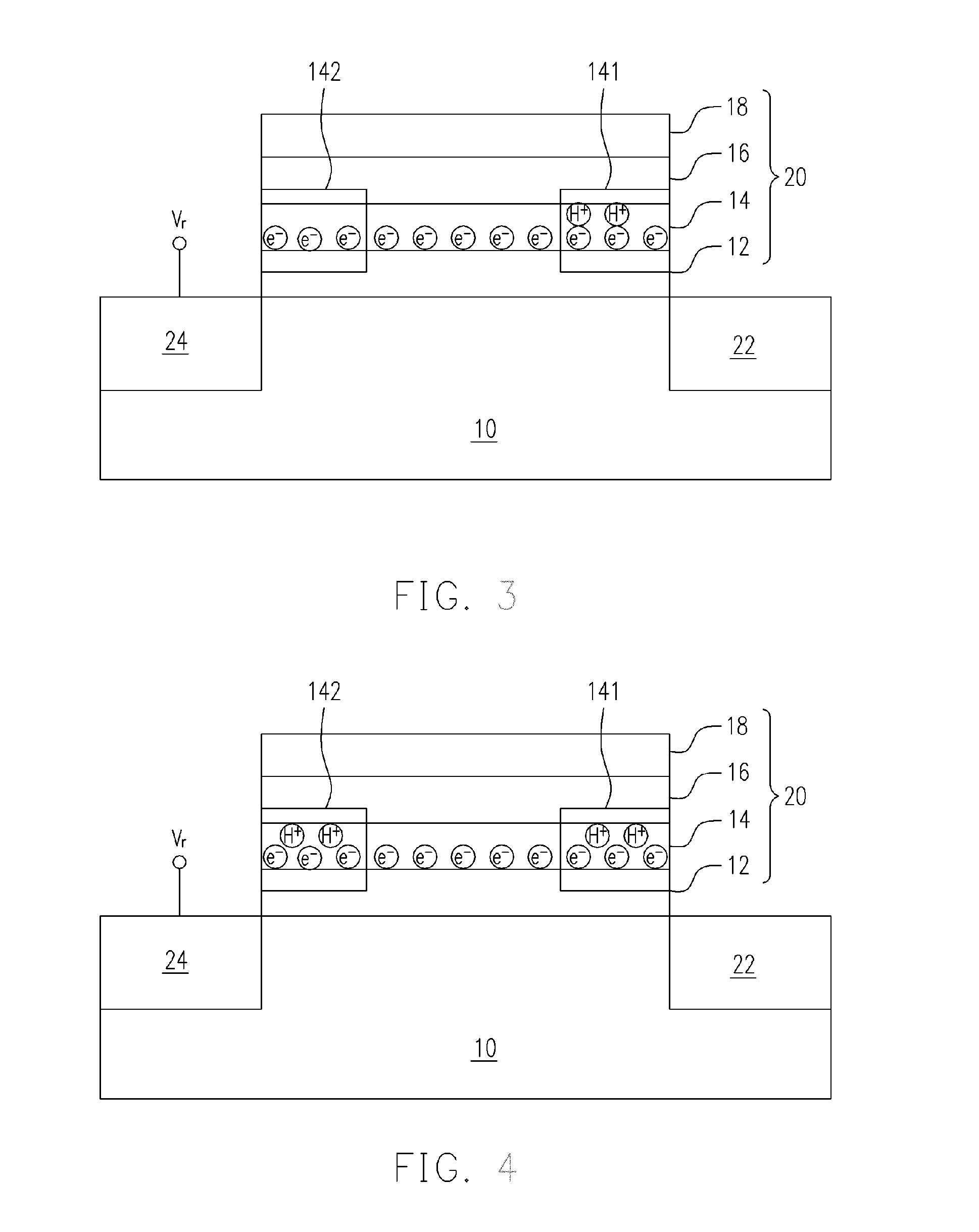
[0026] The illustration of FIG. 1 and FIG. 2 are the operating method for the non-volatile memory of the present invention, where FIG. 1 illustrates the erasing process for the non-volatile memory of the present invention and the FIG. 2 illustrates the programming process for the non-volatile memory of the present invention.
[0027] Referring to FIG. 1, according to the embodiment of the present invention, the non-volatile memory cell comprises at least, a tunneling dielectric layer 12, a charge trapping layer 14, a dielectric layer 16, a gate conducting layer 18, a source region 22 and drain region 24. Where the material for the tunneling dielectric layer 12 is, for example, silicon oxide; the material for the charge trapping layer 14 is, for example, silicon nitride; the material for the dielectric layer 16 is, for example, silicon oxide; and the material for the gate conducting layer 18 is, for example, polysilicon. The tunneling dielectric layer 12, the charge trapping layer 14, ...
PUM
 Abstract
Description
Claims
Application Information
 - R&D Engineer
- R&D Manager
- IP Professional
- Industry Leading Data Capabilities
- Powerful AI technology
- Patent DNA Extraction
Browse by: Latest US Patents, China's latest patents, Technical Efficacy Thesaurus, Application Domain, Technology Topic.
© 2024 PatSnap. All rights reserved.Legal|Privacy policy|Modern Slavery Act Transparency Statement|Sitemap