Semiconductor laser device

a laser device and semiconductor technology, applied in semiconductor lasers, instruments, record information storage, etc., can solve the problems of shortening the lifetime of the device, degrading the end surface, and affecting the performance of the device, so as to increase the light absorption and accelerate the process. , the effect of high power

Active Publication Date: 2007-02-01
NICHIA CORP
View PDF6 Cites 47 Cited by
  • Summary
  • Abstract
  • Description
  • Claims
  • Application Information

AI Technical Summary

Benefits of technology

[0012] With the configuration described above, a layer made of a single crystal material is contained in the first dielectric layer that is directly contacted with the end surface of the resonator of the semiconductor laser device, so that decomposition of the semiconductor layer at the end surface can be prevented. Preferably, the first dielectric layer is made of a single crystal material layer. With this, the efficiency in preventing decomposition can be improved. Further, by having the second dielectric layer including a layer formed of an amorphous on the first dielectric layer, the adhesion between the semiconductor layer and the dielectric layer can be maintained. Preferably, the second dielectric layer is made of an amorphous material.
[0031] As described above, according to the present invention, a high power semiconductor laser device can be provided by preventing the degradation of the end surface of the optical resonator and COD (catastrophic optical damage). COD is a phenomenon by which a crystalline is melted because of light absorption at the end surface of the light emitting side (front) of the device. This occurs when the light is absorbed at interface state of the end surface of the light emitting side (front) of the device, causing the temperature to exceed the melting point of the crystalline, and leading to melting and recrystallization of the semiconductor material at the facets of the laser. COD can be drastically accelerated by light absorption, leading to the increase of temperature, which causes bandgap shrinkage, which in turn causes further increase of light absorption. Thus, COD tends to depend on the output property of the laser device, and can progress easily in the direction of traveling of the light.

Problems solved by technology

Such semiconductor laser devices are required to operate stably for long time in a fundamental mode.
However, when the Al2O3 layer of λ / 2 in thickness is formed with a single layer, an amorphous Al2O3 layer may react with the semiconductor device under high output drive of 300 mW or higher, which leads to degradation of the end surfaces.
Also, in the semiconductor laser devices using the nitride semiconductors, if the dielectric layer of the end surface of the light emitting side is made of a single layer, destruction of the end surface tends to occur under high output operation such as at 30 mW or higher, resulting in a shortening the lifetime of the device.
Moreover, in high output driving, the driving current becomes too large when the slope efficiency is low.
When the greater current is applied, heat can be generated at the laser device, and the heat can degrade or destroy the crystal.

Method used


Image

  • Semiconductor laser device
  • Semiconductor laser device
  • Semiconductor laser device

Examples


example 1

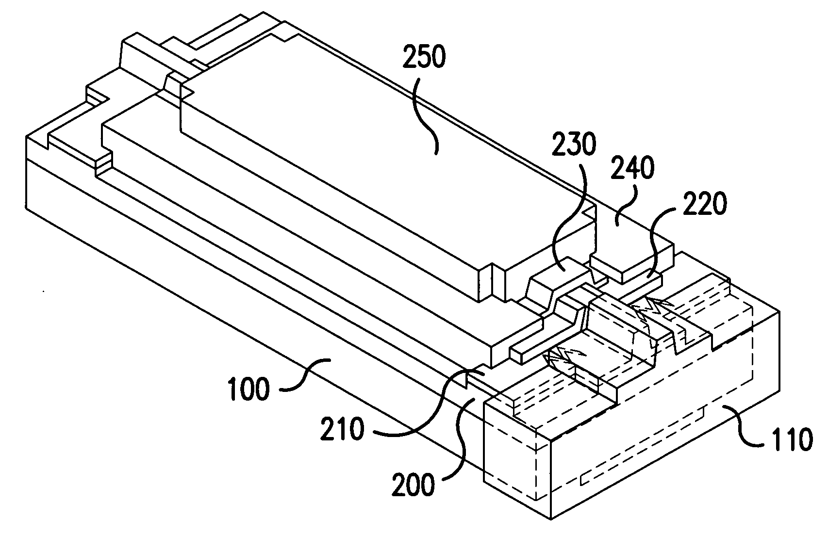
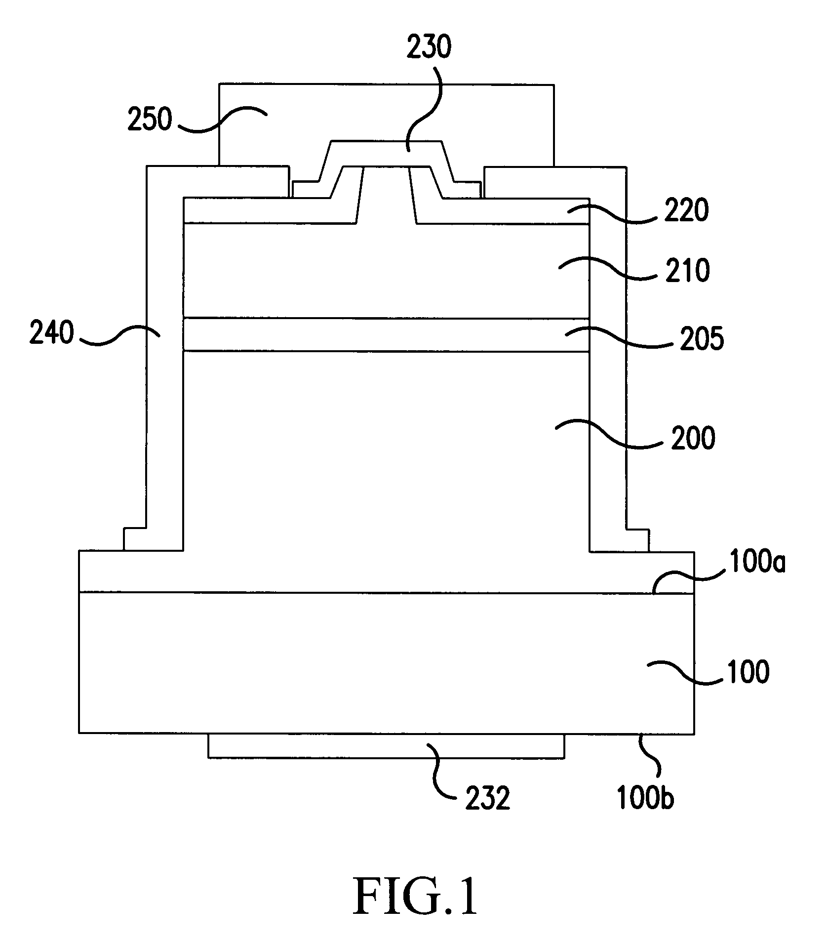
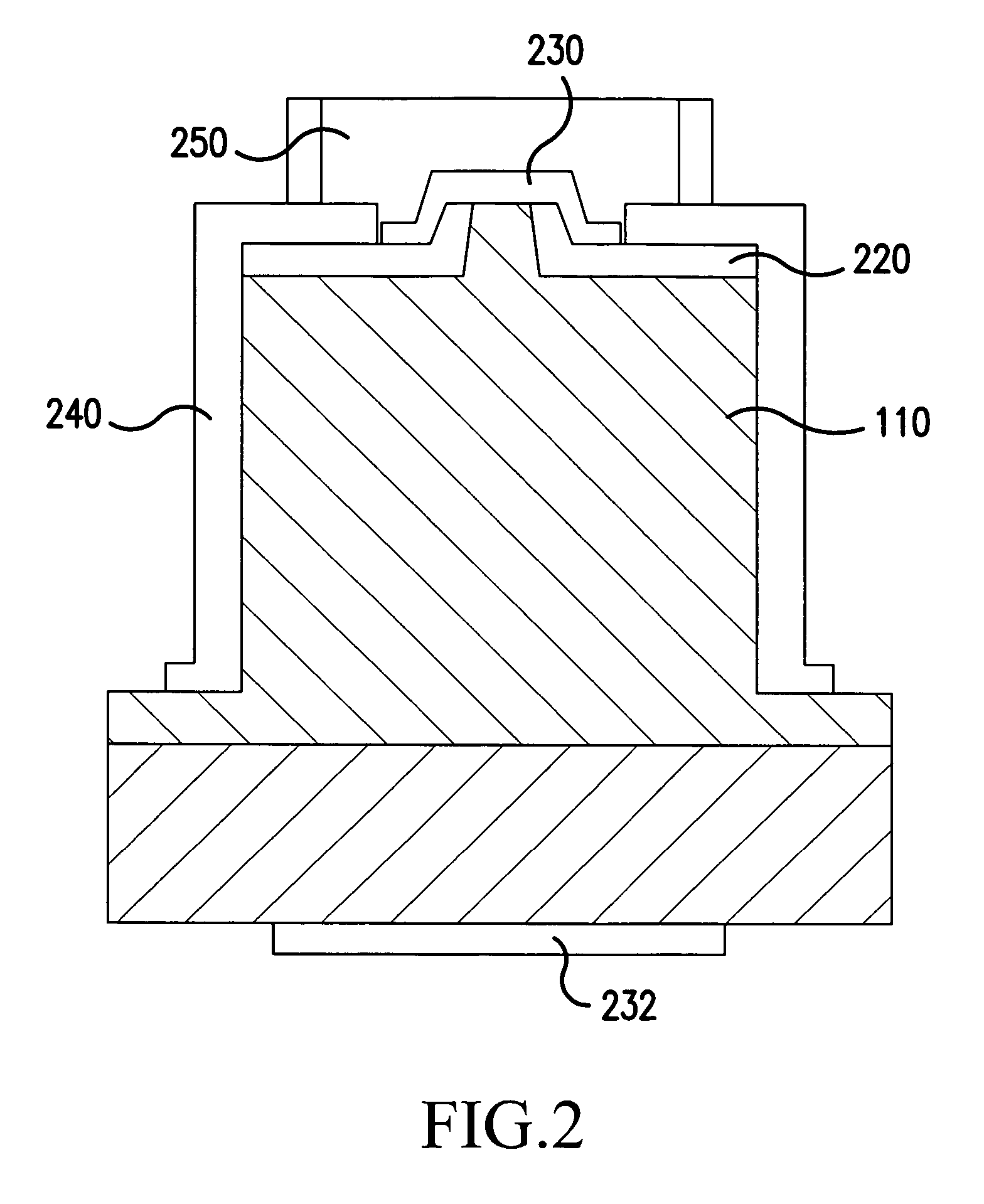
[0092] For the substrate, a wafer-shaped GaN substrate 100 whose main surface is C-plane is used. The substrate is not specifically limited to the above and a GaN substrate whose main surface is R-plane or A-plane can be used according to need.

(n-Type Cladding Layer 201)

[0093] Next, the GaN substrate is fed into a MOCVD apparatus. At the atmospheric temperature in the furnace of 1050° C., using TMA (trimethylaluminum), TMG (trimethylgallium) and ammonia as the raw material gases, an n-type cladding layer of undoped Al0.04Ga0.96N is grown to the thickness of 2.0 μm on the GaN substrate.

(n-Type Optical Guide Layer 202)

[0094] Next, at approximately the same temperature as in growing the n-type cladding layer and using TMG and ammonia as the raw material gases, an n-type optical guide layer of undoped GaN is grown to a thickness of 0.19 μm. This layer may be doped with an n-type dopant.

(Active Layer 205)

[0095] Next, at the temperature of 800° C. and using TMI, TMG and ammonia a...

example 2

[0110] A nitride semiconductor laser device is fabricated in a similar manner as in Example 1, except that the dielectric film 110 of the end surface of the light emitting side is constructed as below. A ECR sputtering apparatus is used. After cleaning the end surface of the light emitting side by using plasma of an active gas such as oxygen, a first dielectric layer and a second dielectric layer made of AlxOy are formed. First, the first dielectric layer is disposed to a thickness of 20 nm by using the metal target of 5N Al, under the conditions of the Ar flow rate 15 sccm, the O2 flow rate of 10 sccm, the microwave power of 600W, and the RF of 600 W. Then, using the metal target of 5N Al, the second dielectric layer is disposed to a thickness of 100 nm, under the conditions of the Ar flow rate 10 sccm, the O2 flow rate of 3 sccm, the microwave power of 450 W, and the RF of 450 W. In this case, the refractive index of the first dielectric layer to the light with a wavelength of 405...

example 3

[0111] A nitride semiconductor laser device is fabricated in a similar manner as in Example 1, except that the dielectric film is constructed as below.

[0112] The end surface of the light emitting side is cleaned by using ECR sputtering apparatus with plasma of an active gas such as oxygen, using 5N Al as the metal target and under the conditions of Ar flow rate 15 sccm, the O2 flow rate 10 sccm, the microwave power 600 W, and the RF 600 W, a first dielectric layer 111 is disposed to a thickness of 20 nm and then, using 5N Al as the metal target and under the conditions of Ar flow rate 10 sccm, the O2 flow rate 3 sccm, the microwave power 450 W, and the RF 450 W, a second dielectric layer is disposed to a thickness of 40 nm to form a dielectric film 110. In this case, the refractive index of the first dielectric layer to the light with a wavelength of 405 nm is 1.63 and the refractive index of the second dielectric layer is 1.67.

[0113] Thereafter, a Al2O3 layer is disposed to a thi...


PUM

PropertyMeasurementUnit
reflectanceaaaaaaaaaa
oscillation wavelengthaaaaaaaaaa
reflectanceaaaaaaaaaa

Abstract

A semiconductor laser device, which has a protective film at an end surface thereof, is adaptable to demands for higher outputs or shorter wavelengths. The semiconductor laser device according to the present invention includes a dielectric film on at least one end surface of an optical resonator, in which the dielectric film includes a first dielectric layer and a second dielectric layer comprised of the same elements and disposed in sequence from the end surface side of the semiconductor, the first dielectric layer including a layer made of a single crystal material and the second dielectric layer including a layer made of an amorphous material.

Description

[0001] This application claims priority from the applications No. 2005-221338 filed in Japan on Jul. 29, 2005, the contents of which are incorporated hereinto by reference. BACKGROUND OF THE INVENTION [0002] 1. Field of the Invention [0003] The present invention relates to a semiconductor laser device, in particular, to a high output semiconductor laser device whose oscillation wavelength is 600 nm or less. [0004] 2. Description of the Related Art [0005] Presently, high output semiconductor laser devices are in demand for use in writing onto optical discs and magnetic optical discs. Such semiconductor laser devices are required to operate stably for long time in a fundamental mode. [0006] Also, in order to realize the shorter wavelengths necessary for higher recording density of optical discs, semiconductor laser devices using nitride semiconductors have been researched. The laser devices using the nitride semiconductors can be applied not only as a light source for optical discs, b...

Claims


Application Information

Patent Timeline
Patent Type & Authority Applications(United States)
IPC IPC(8): G11B7/00
CPCB82Y20/00H01S5/028H01S5/34333H01S5/0287H01S5/16H01S5/0282H01S5/30
Inventor OCHIAI, MASANAOYUASA, KOJI
Owner NICHIA CORP
Why Eureka
Try Eureka