Multilayer printed wiring board

a printed wiring and multi-layer technology, applied in the direction of printed element electric connection formation, high-current circuit adaptation, semiconductor/solid-state device details, etc., can solve the problems of high ic chip often turns inoperative, and increase the frequency of occurrence of malfunction or error. , to achieve the effect of improving the electric characteristic, reducing the total inductance, and easy matching

Active Publication Date: 2007-02-08
IBIDEN CO LTD
View PDF11 Cites 71 Cited by
  • Summary
  • Abstract
  • Description
  • Claims
  • Application Information

AI Technical Summary

Benefits of technology

[0041] At this time, preferably, two or more layers of the GND layers or VCC layers are formed and the GND layer and the VCC layer are disposed alternately. The thickness of each insulating layer between respective conductive layers is preferred to be substantially equal. The reason is that because operations of reducing both inductances are executed uniformly, total inductance can be reduced easily. Further, impedance is easy to match so as to improve the electric characteristic.
[0042] What is more preferable is that there are provided two or more VCC layers and GND layers. As a result, the GND layer and the VCC layer disposed in the inner layer reduces mutual inductance as compared with the surface portion. The effect appears more conceivably.
[0043] A distance between the GND layer and the VCC layer is preferred to be in the range of 25 to 400 μm. If it is less than 25 μm, it is likely difficult to secure insulation characteristics regardless of material. If reliability test such as porosity test is carried out, short-circuit can occur between conductive layers. If it exceeds 400 μm, the effect of reducing inductance is reduced. That is, because of such a distance, the effect of mutual inductance is cancelled out.
[0044] For both the GND layer and the VCC layer, it is preferable to increase the thickness of their conductive layers. The reason is that by increasing both the volumes, the effect of reduction of resistance is easy to

Problems solved by technology

However, as the frequency of an IC chip is higher, the noise of occurrence of becomes higher.
Particularly if the frequency of the IC chip exceeds 3 GHz, the frequency of occurrence of malfunction or error considerably increases.
If the frequency exceeds 5 GHz, the IC chip often turns inoperative.
Due to this, it cannot perform operations that the computer should do, i.e., cannot perform desired functions and operations such as

Method used


Image

  • Multilayer printed wiring board
  • Multilayer printed wiring board
  • Multilayer printed wiring board

Examples


second embodiment

[Second Embodiment] 3-Layer Multi-Layer Core Substrate

[0127] The multi-layer printed wiring board according to the second embodiment will be described with reference to FIG. 13.

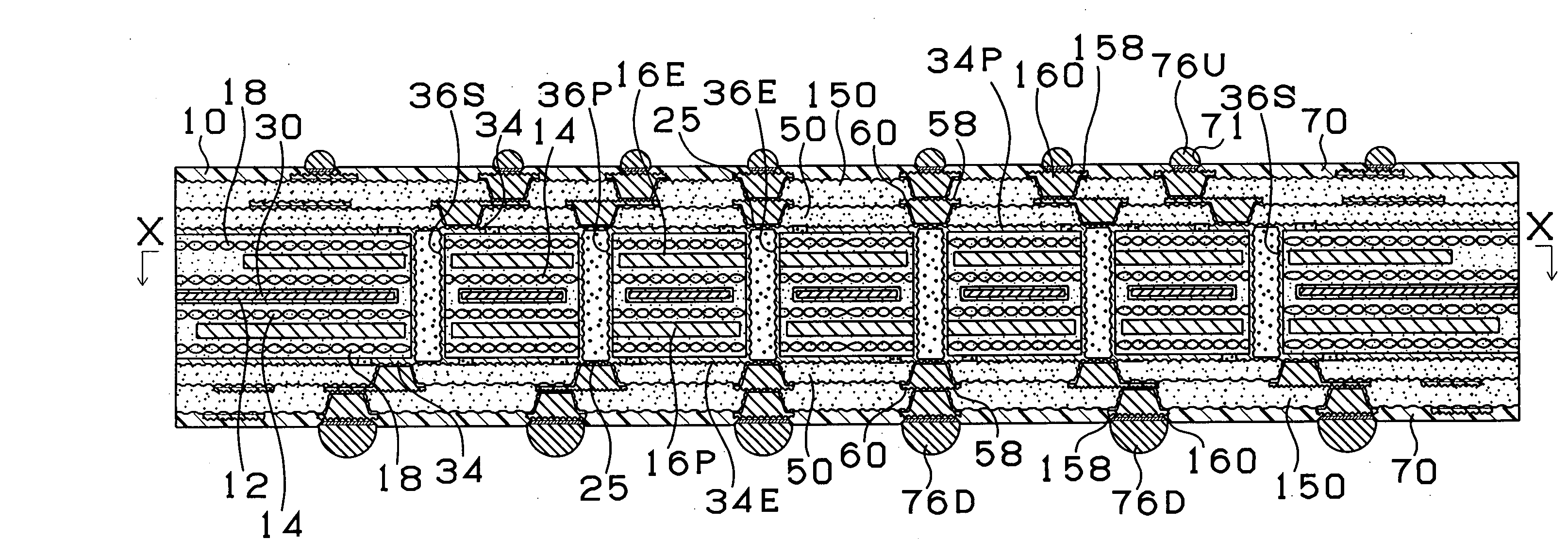
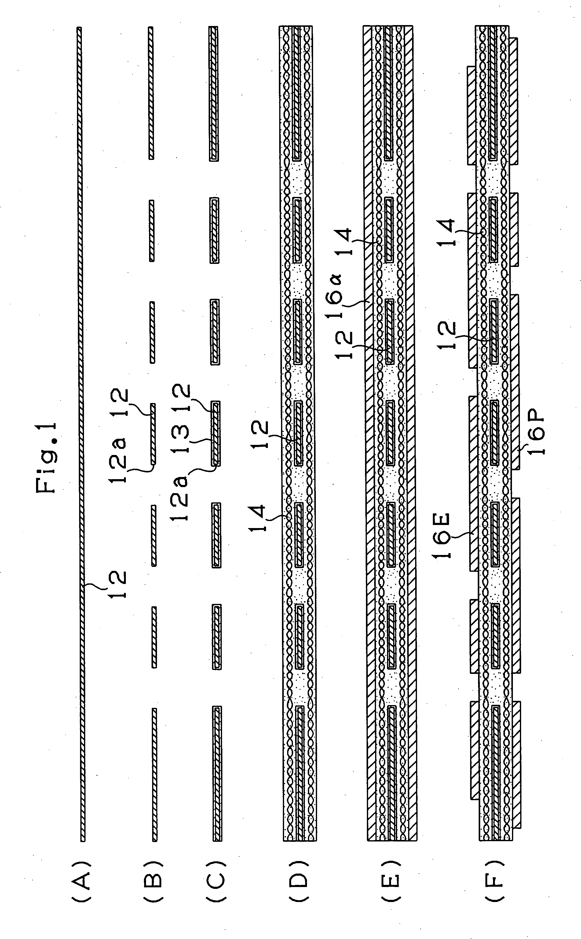
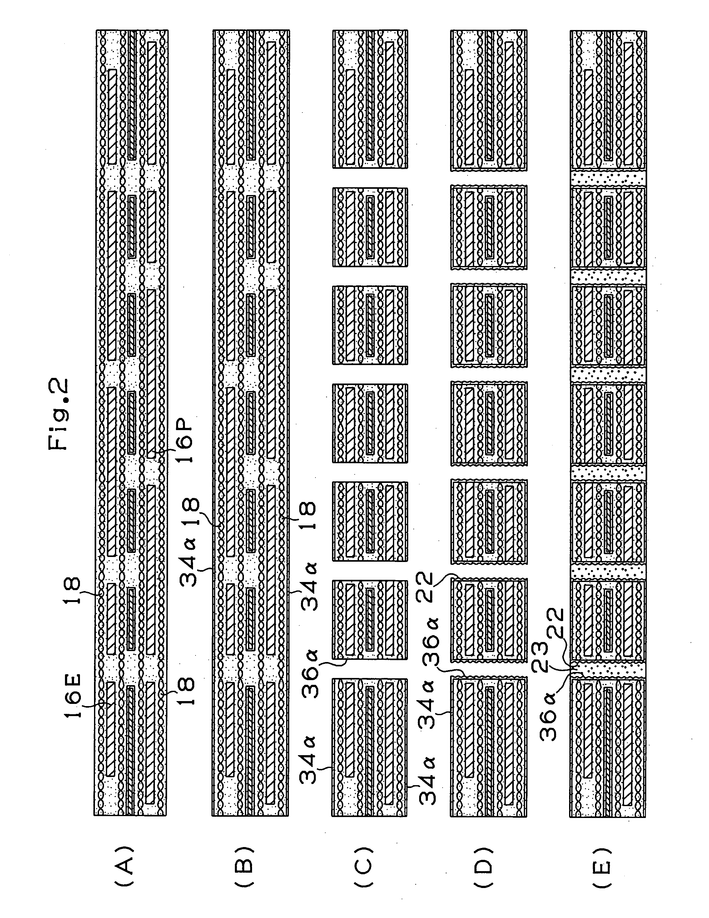
[0128] According to the first embodiment described with reference to FIG. 8, the core substrate is composed of four layers (ground layers 16E, 34E:2, power layers 16P, 34P:2). Contrary to this, according to the second embodiment, as shown in FIG. 13, the multi-layer core substrate 30 is composed of three layers (ground layers 34E, 34E:2, power layer 15P:1).

[0129] In the multi-layer printed wiring board 10 according to the second embodiment, as shown in FIG. 13, the conductor circuit 34 and the ground conductive layer 34E are formed on each of the front surface and the rear surface of the multi-layer core substrate 30 and the power conductive layer 15P is formed inside the core substrate 30. The ground conductive layer 34E is formed as a ground plain layer and the power conductive layer 15P is formed as a po...

third embodiment

[Third Embodiment] Glass Epoxy Resin Substrate

[0135] Although in the first and second embodiments, the multi-layer core substrate 30 is employed, according to the third embodiment, a single core substrate 30 is used as shown in FIG. 15 and the conductive layers on both sides of the core substrate are formed as the power layer and ground layer. That is, the ground layer 34E is formed on top of the core substrate 30 and the power layer 34P is formed on the bottom thereof. The front surface and rear surface of the core substrate 30 are connected via the power through hole 36P, the ground through hole 36E and the signal through hole 36S. Above the conductive layers 34P, 34E are disposed the interlayer resin insulating layer 50 in which the via hole 60 and the conductive layer 58 are formed and the interlayer resin insulating layer 150 in which the via hole 160 and the conductor circuit 158 are formed.

[0136] According to the third embodiment also, like the first embodiment described wit...


PUM


Abstract

In a core substrate 30, a ground through hole 36E and a power through hole 36P are disposed in the grid formation, so that electromotive force induced in X direction and Y direction cancel out each other. As a result, even if mutual inductance is reduced and a high frequency IC chip is loaded, electric characteristic and reliability can be improved without generating malfunction or error.

Description

TECHNICAL FIELD [0001] This invention relates to a multilayer printed wiring board and provides a technique related to a multilayer printed wiring board capable of having improved electric characteristics and reliability without causing malfunction, error or the like even if a high frequency IC chip, particularly an IC chip in a high frequency range of 3 GHz or higher is mounted thereon. BACKGROUND ART [0002] In forming a buildup type multilayer printed wiring board constituting an IC chip package, interlayer insulating resin is formed on one of or each of the surfaces of a core substrate having through holes formed therein and via holes for interlayer conduction are opened by a laser or photo etching, whereby an interlayer resin insulating layer is thereby formed. A conductor layer is formed on the via holes by plating or the like and etching and the like are performed to form a pattern, thus creating a conductor circuit. Further, by repeatedly forming the interlayer insulating lay...

Claims


Application Information

Patent Timeline
IPC IPC(8): H05K1/11H01L23/498H01L23/50H05K3/42H05K3/46
CPCH01L23/49822H01L2224/16235H01L23/50H01L2224/16H01L2924/01025H01L2924/01046H01L2924/01078H01L2924/01079H01L2924/09701H01L2924/15311H01L2924/15312H01L2924/19106H01L2924/3011H05K1/0263H05K1/115H05K3/429H05K3/4602H05K3/4608H05K3/4641H05K2201/09309H05K2201/09536H05K2201/0959H05K2201/09609H01L2924/01019H01L2224/16225H01L23/49838H01L2224/05573H01L2224/05568H01L2924/00014H01L2224/0554H01L2224/05599H01L2224/0555H01L2224/0556H05K3/46
Inventor KATO, SHINOBU
Owner IBIDEN CO LTD
Why Eureka
Try Eureka