Nanowire based non-volatile floating-gate memory

a technology of floating-gate memory and nanowires, which is applied in the direction of nanotechnology, electrical equipment, semiconductor devices, etc., can solve the problem of decoupling the size of each of the nanowires from its density, and achieve good size and shape control, high-quality control

Inactive Publication Date: 2007-02-08
IBM CORP
View PDF4 Cites 45 Cited by
  • Summary
  • Abstract
  • Description
  • Claims
  • Application Information

AI Technical Summary

Benefits of technology

[0009] The use of nanowires as nanocrystals has the following advantages: First, nanowire growth provides good size and shape control. Second, the nanowires formed utilizing the inventive methods are single-crystal with a well-defined orientation. Third, the size of each of the nanowires is decoupled from their den

Problems solved by technology

Third, the size of each of the nanow

Method used


Image

  • Nanowire based non-volatile floating-gate memory
  • Nanowire based non-volatile floating-gate memory
  • Nanowire based non-volatile floating-gate memory

Examples


Embodiment Construction

[0018] The present invention, which discloses a nanowire-based non-volatile memory as well as methods for forming the same, will now be described in greater detail by referring to the following discussion. In this discussion, reference will be made to various drawings that illustrate embodiments of the present invention. Since the drawings of the embodiments of the present invention are provided for illustrative purposes, the structures contained therein are not drawn to scale.

[0019] It is noted that the discussion that follows is described for making Si-containing nanowires and silicon-containing processing. The methods of the present invention can also be produced with other semiconductors such as Ge or III-V compound semiconductors. Use of Si-containing semiconductors such as, for example, Si, SiGe, Si / SiGe, silicon-on-insulator (SOI), silicon germanium-on-insulator (SGOI), SiC or SiGeC are, however, preferred.

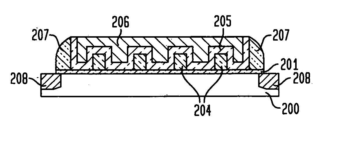
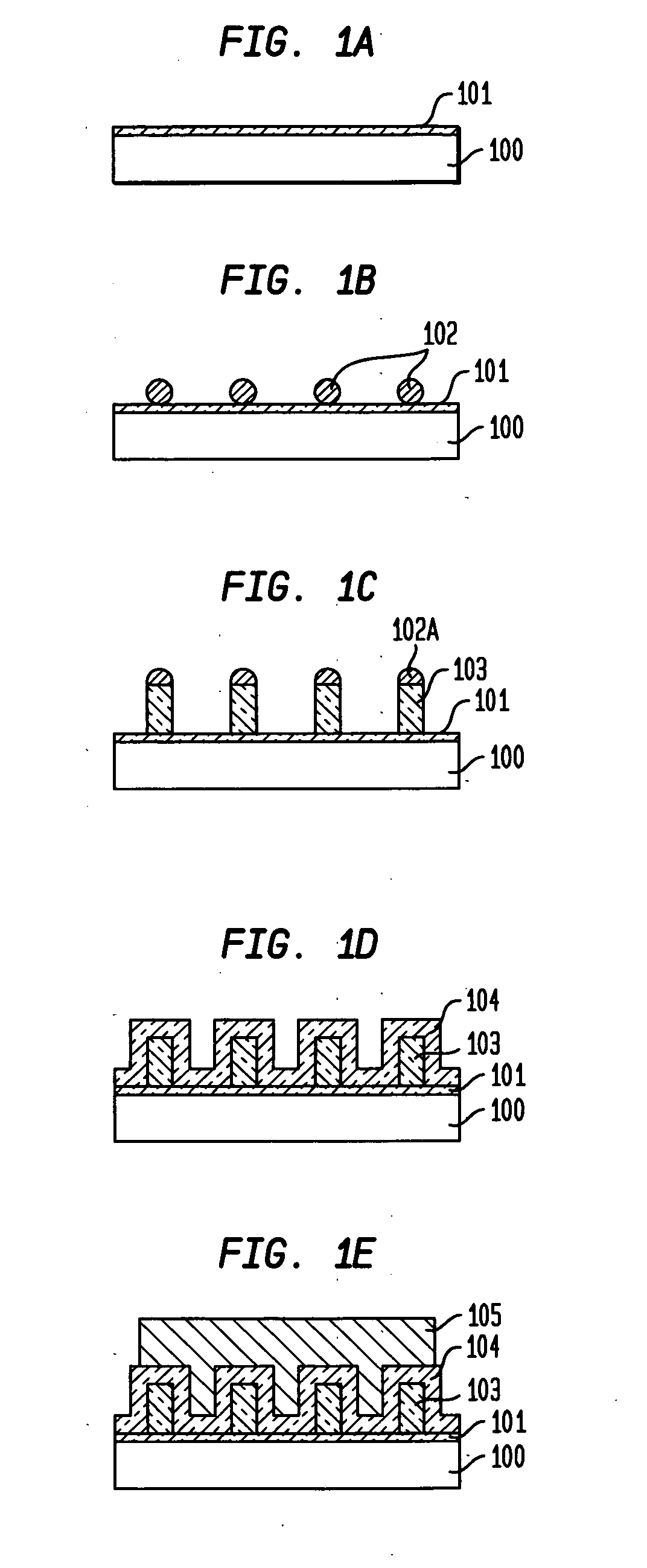
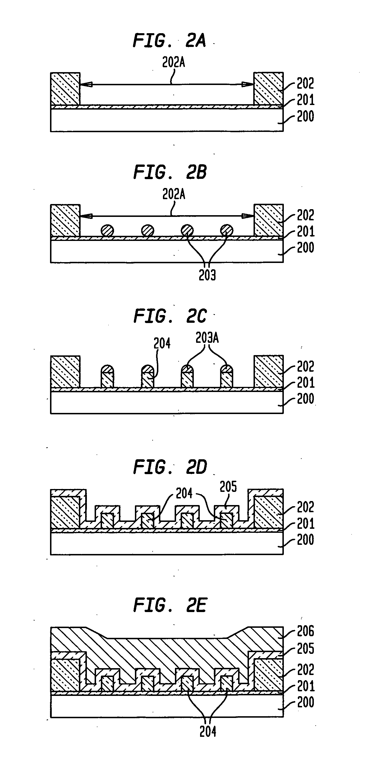
[0020] The basic method is shown in FIGS. 1A-1E. A silicon-containin...


PUM


Abstract

A non-volatile memory transistor with a nanocrystal-containing floating gate formed by nanowires is disclosed. The nanocrystals are formed by the growth of short nanowires over a crystalline program oxide. As a result, the nanocrystals are single-crystals of uniform size and single-crystal orientation.

Description

RELATED APPLICATION [0001] This application is related to co-pending and co-assigned U.S. Patent Application Publication No. 2004 / 0256662 A1, publication date Dec. 23, 2004, which application has signed as U.S. Ser. No. 10 / 465,797, filed Jun. 20, 2003.FIELD OF THE INVENTION [0002] The present invention relates to electronic devices based on semiconductor nanowires, and more particularly to a floating-gate non-volatile memory which includes nanocrystals (i.e., nanocrystal-based floating-gate non-volatile memory) and methods of fabricating such a memory. BACKGROUND OF THE INVENTION [0003] When compared with conventional floating-gate memories, floating-gate memories that are based on nanocrystals have the following advantages: (1) They are less susceptible to defects in the program oxide since the charge is stored on isolated nanocrystal sites. (2) They can store two bits per cell by reversing the role of the source and drain since the charge is localized at the injection point. (3) T...

Claims


Application Information

Patent Timeline
IPC IPC(8): H01L29/788
CPCB82Y10/00H01L21/28273H01L29/42332H01L29/7881H01L29/7887Y10S977/814H01L29/0676Y10S977/762Y10S977/891Y10S977/943Y10S977/832H01L29/94H01L29/40114
Inventor COHEN, GUY M.
Owner IBM CORP
Why Eureka
Try Eureka