Regulated Capacitive Loading and Gain Control of a Crystal Oscillator During Startup and Steady State Operation

a crystal oscillator and capacitive loading technology, applied in the field of crystal oscillator circuits, can solve the problems of large resistance of the circuit, achieve the effects of reducing capacitive loading, increasing negative resistance, and speeding up startup conditions

Inactive Publication Date: 2007-02-08
MONTEREY RES LLC
View PDF14 Cites 28 Cited by
  • Summary
  • Abstract
  • Description
  • Claims
  • Application Information

AI Technical Summary

Benefits of technology

[0012] The problems outlined above are in large part solved by an improved oscillator circuit that preferably includes a piezoelectric material such as a quartz crystal. The improved oscillator includes circuitry which monitors the oscillator output. Depending on, for example, the amplitude of that output relative to a reference, the oscillator includes further circuitry that can change the capacitive loading and/or amplifier gain as seen by the oscillator. For example, during a startup mode, it would be desirable to reduce the capacitive loading seen by the crystal and to increase the amount of negative resistance provided by the circuit. This can provi

Problems solved by technology

Moreover, when the load capacitors are large,

Method used


Image

  • Regulated Capacitive Loading and Gain Control of a Crystal Oscillator During Startup and Steady State Operation
  • Regulated Capacitive Loading and Gain Control of a Crystal Oscillator During Startup and Steady State Operation
  • Regulated Capacitive Loading and Gain Control of a Crystal Oscillator During Startup and Steady State Operation

Examples


Embodiment Construction

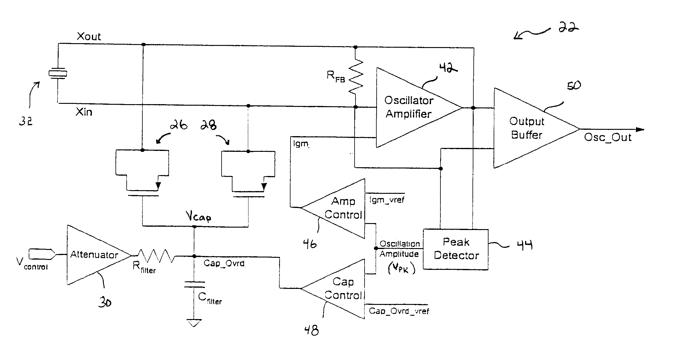
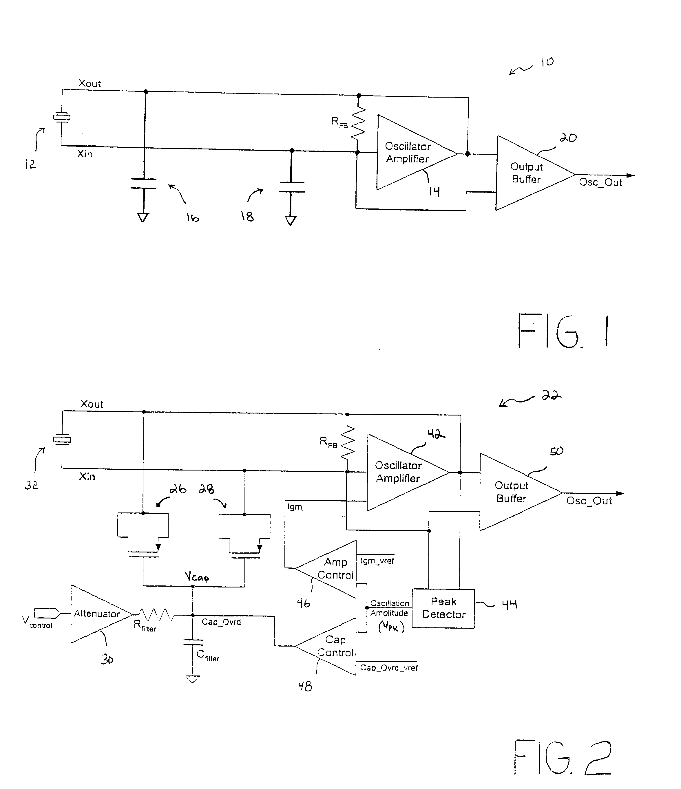
[0026] Turning now to the drawings, FIG. 1 illustrates one form of an oscillator 10 having a piezoelectric resonator 12. Oscillator 10 may include either an inverter or, as shown, an amplifier 14 placed between nodes of the resonator 12. A feedback resistor RFB can also be connected between oscillator nodes to bias the nodes to an appropriate voltage differential. The frequency of oscillation can be varied if needed by adjusting capacitance values within capacitors 16 and 18 coupled, respectively, to nodes Xout and Xin. The capacitors can be modified in value to possibly pull the frequency of the oscillator. Rather than having to change out the capacitors each time the oscillator frequency must be changed, capacitors 16 and 18 are preferably voltage-variable capacitors or varactors. Varactors used in this way also allow the oscillation frequency to be controlled by the varactor control voltage to from a voltage controlled crystal oscillator (VCXO). There are many ways in which a var...


PUM


Abstract

An oscillator circuit and system are provided having a peak detector that can determine a peak voltage value from the oscillator. The peak voltage value can then be compared against a predetermined voltage value by a controller coupled to the peak detector. The comparison value is then used to change a bias signal if the peak voltage value is dissimilar from the predetermined voltage value. A variable capacitor or varactor can be formed from a transistor and is coupled to the oscillator for receiving the bias signal upon a varactor bias node. The bias signal is used to regulate the capacitance within the varactor as applied to the oscillator nodes. Another controller can also be coupled to the peak detector to produce a second bias signal if the peak voltage is dissimilar from a second predetermined voltage value. The second bias signal can then be forwarded into an amplifier having a variable gain to regulate the gain applied to the oscillator. The combination of a varactor and variable gain amplifier regulate the negative resistance applied to the resonating circuit during startup and steady state operations to ensure a relatively fast startup, and to maintain optimal loading and accurate steady state amplitude after startup has completed.

Description

PRIORITY CLAIM [0001] This application claims priority to U.S. Provisional Application No. 60 / 665,465 entitled “Crystal Oscillator Capacitor Override,” filed Mar. 24, 2005.BACKGROUND OF THE INVENTION [0002] 1. Field of the Invention [0003] The present invention relates to an oscillator and, more specifically, to a crystal oscillator circuit having a regulated capacitive loading and regulated amplifier gain to optimize both startup and steady state operation of the crystal oscillator. [0004] 2. Description of the Related Art [0005] The following descriptions and examples are not admitted to be prior art or conventional by virtue of their inclusion within this section. [0006] Within nearly every electronic subsystem is some form of generator that produces cyclical waveforms. The waveform generator is oftentimes referred to as an oscillator. Depending on the application, an oscillator can be used simply as a source of regularly spaced pulses or clock signals. There are numerous types o...

Claims


Application Information

Patent Timeline
IPC IPC(8): H03B5/12H03C3/22H03B5/18
CPCH03B5/06H03B5/36H03B5/368H03B2200/0046H03L5/00H03B2200/0062H03B2200/0094H03L3/00H03B2200/005
Inventor BRENNAN, AARONMCMENAMY, MIKE
Owner MONTEREY RES LLC
Why Eureka
Try Eureka