
Systems Configured to Generate Output Corresponding to Defects on a Specimen

a technology of output and specimen, applied in the direction of polarisation-affecting properties, phase-affecting property measurements, instruments, etc., can solve the problems of amplitude perturbation and complex field resulting from defects that are significantly weaker compared to current inspection systems, and the need for detection of defects of decreasing size has become necessary. , to achieve the effect of increasing contrast and low resolution

Inactive Publication Date: 2007-02-08
KLA TENCOR TECH CORP
View PDF3 Cites 35 Cited by
  • Summary
  • Abstract
  • Description
  • Claims
  • Application Information

AI Technical Summary

Benefits of technology

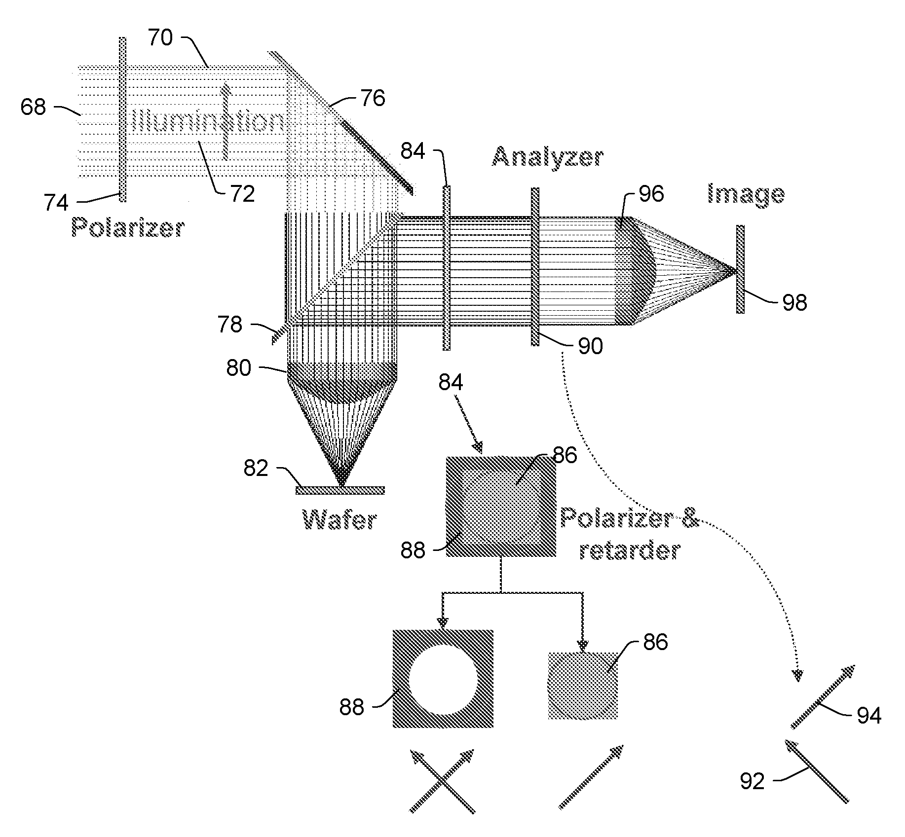
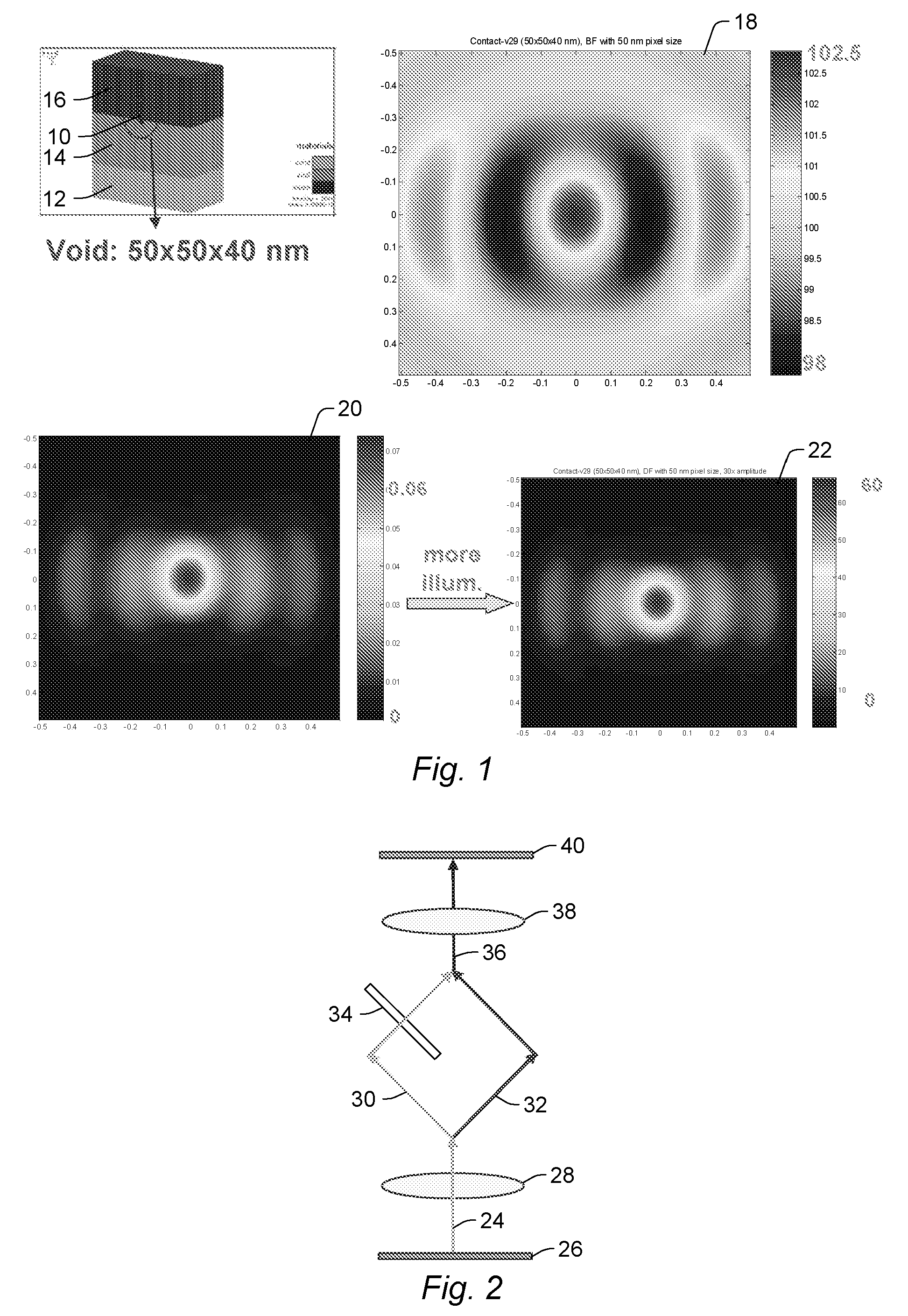
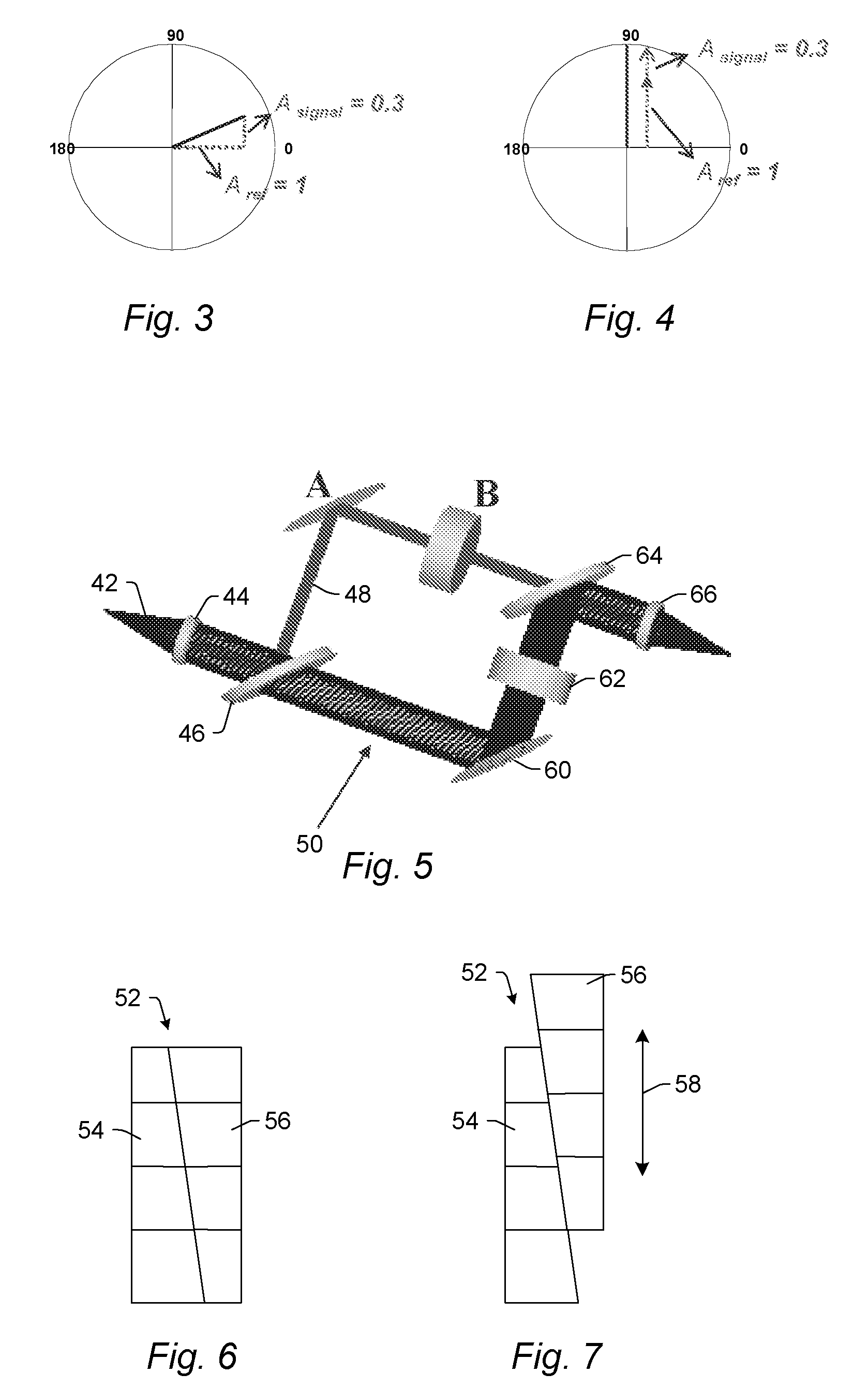
[0014] The above-described system may also, therefore, be used for interference contrast enhancement. In some such embodiments, the system may be configured for “axial” differential interference contrast (DIC), in which the reference beam is used as a “low resolution copy” of the test beam. For example, in one embodiment, the reference beam and the test beam are reflected from the same measurement spot on the specimen. In one such embodiment, the reference beam has a lower resolution than the test beam. In another embodiment, the reference beam and the test beam have different imaging pupil profiles. In a preferred embodiment, the reference beam is oriented such that the phase of the reference beam is substantially parallel to the phase of a portion of the test beam reflected from the defects. For example, in some embodiments, the system is configured to adjust the reference beam such that the reference beam can be oriented to be in-phase with a portion of the test beam reflected from the defects to increase the contrast.

Problems solved by technology

For instance, as the dimensions of semiconductor devices decrease, detection of defects of decreasing size has become necessary since even relatively small defects may cause unwanted aberrations in the semiconductor devices.
There are, however, many disadvantages to currently used inspection systems.
For instance, as design rules shrink, the amplitude perturbations and complex fields resulting from defects are significantly weaker compared to those resulting from the object being inspected.
With BF mode, because of the small amplitude perturbations, the contrast of the defect image is relatively low making the defect extremely difficult to detect.
For DF mode, the defect contrast is generally satisfactory; however, the raw signal is typically so weak that the signal is not above the sensor noise.
However, to increase the DF signal to useful levels, the required increase in the illumination level is impractical due to source availability or wafer damage risk.
Currently, defect inspection based on phase detection using the spatial fringe technique is susceptible to system noise, has higher costs for image processing, and is limited by the sampling of the fringe.
Therefore, these systems and methods will be particularly susceptible to noise such as that caused by system vibration and variations in focus at the different positions on the target.
In addition, as described in these publications, relatively complex image processing techniques are used to reduce the non-defective aberrations between the images being compared.
The image processing techniques not only increase cost and reduce throughput, but more importantly may undesirably alter the image data such that defects, and particularly defects of relatively small size, are detected with less accuracy.

Method used


Image

  • Systems Configured to Generate Output Corresponding to Defects on a Specimen
  • Systems Configured to Generate Output Corresponding to Defects on a Specimen
  • Systems Configured to Generate Output Corresponding to Defects on a Specimen

Examples


Embodiment Construction

[0043] As used herein, the term “defect” generally refers to any abnormality that may be formed on or within any specimen described herein.

[0044] As used herein, the term “specimen” generally refers to a wafer or a reticle (or “mask”). As used herein, the term “wafer” generally refers to substrates formed of a semiconductor or non-semiconductor material. Examples of such a semiconductor or non-semiconductor material include, but are not limited to, monocrystalline silicon, gallium arsenide, and indium phosphide. Such substrates may be commonly found and / or processed in semiconductor fabrication facilities. A wafer may include one or more layers formed upon a substrate. For example, such layers may include, but are not limited to, a resist, a dielectric material, and a conductive material. Many different types of such layers are known in the art, and the term wafer as used herein is intended to encompass a wafer including all types of such layers.

[0045] One or more layers formed on...


PUM


Abstract

Systems configured to generate output corresponding to defects on a specimen and systems configured to generate phase information about defects on a specimen are provided. One system includes an optical subsystem that is configured to create interference between a test beam and a reference beam. The test beam and the reference beam are reflected from the specimen. The system also includes a detector that is configured to generate output representative of the interference between the test and reference beams. The interference increases contrast between the output corresponding to the defects and output corresponding to non-defective portions of the specimen.

Description

PRIORITY CLAIM [0001] This application claims priority to U.S. Provisional Application No. 60 / 704,738 entitled “Systems Configured to Generate Signals Corresponding to Defects on a Wafer,” filed Aug. 2, 2005, which is incorporated by reference as if fully set forth herein.BACKGROUND OF THE INVENTION [0002] 1. Field of the Invention [0003] This invention generally relates to systems configured to generate output corresponding to defects on a specimen. Certain embodiments relate to systems that include an optical subsystem that is configured to create interference between a test beam and a reference beam, both of which are reflected from a specimen. [0004] 2. Description of the Related Art [0005] The following description and examples are not admitted to be prior art by virtue of their inclusion in this section. [0006] Fabricating semiconductor devices such as logic and memory devices typically includes processing a substrate such as a semiconductor wafer using a number of semiconduct...

Claims


Application Information

Patent Timeline
IPC IPC(8): G01N21/00
CPCG01N21/21G01N21/9501G01N21/45
Inventor HWANG, SHIOW-HWEIFU, TAO-YILIU, XIUMEI
Owner KLA TENCOR TECH CORP
Learn More