

Mosaic diamond substrates
a diamond substrate and mosaic diamond technology, applied in the field ofmosaic diamond substrates, can solve the problems of low break down voltage, high leakage current and low break down voltage of semiconductors, and decrease in the size of semiconductor transistors and other circuit elements, so as to improve the quality of diamond growth and high temperature
- Summary
- Abstract
- Description
- Claims
- Application Information
AI Technical Summary
Benefits of technology
Problems solved by technology
Method used
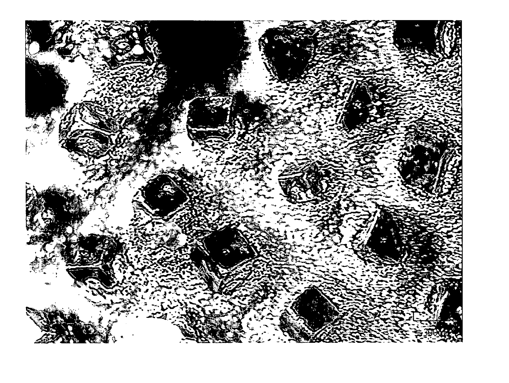
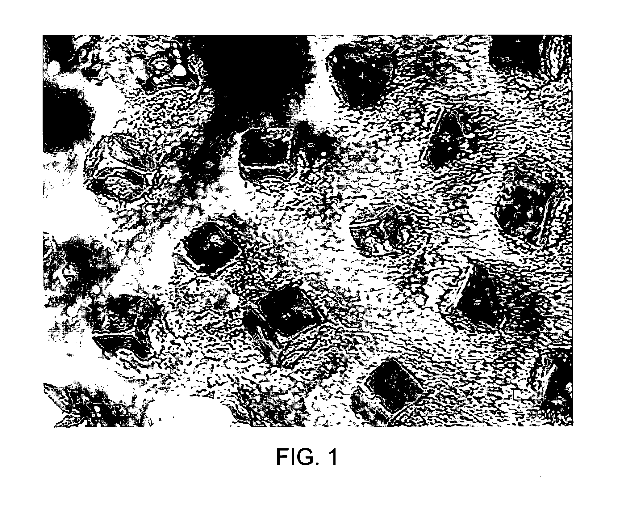
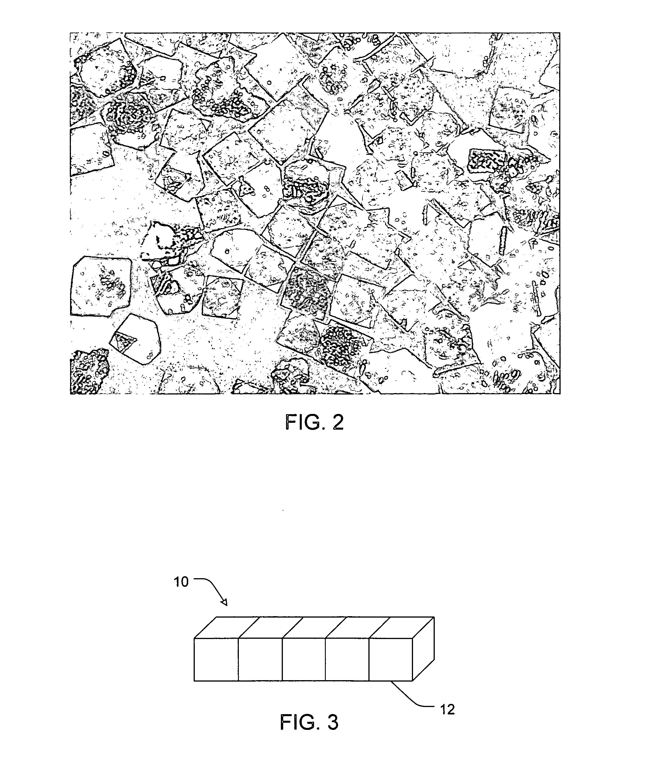
Image

Examples
Embodiment Construction
[0024] Before the present invention is disclosed and described, it is to be understood that this invention is not limited to the particular structures, process steps, or materials disclosed herein, but is extended to equivalents thereof as would be recognized by those ordinarily skilled in the relevant arts. It should also be understood that terminology employed herein is used for the purpose of describing particular embodiments only and is not intended to be limiting.
[0025] The singular forms “a,”“an,” and “the” include plural referents unless the context clearly dictates otherwise. Thus, for example, reference to “a diamond segment” includes reference to one or more of such segments, and reference to “a high pressure apparatus” includes reference to one or more of such devices.
[0026] Definitions
[0027] In describing and claiming the present invention, the following terminology will be used in accordance with the definitions set forth below.
[0028] As used herein, the term “one d...
PUM
| Property | Measurement | Unit |
|---|---|---|
| Length | aaaaa | aaaaa |
| Thickness | aaaaa | aaaaa |
| Thickness | aaaaa | aaaaa |
Abstract
Description
Claims
Application Information