Semiconductor device and a manufacturing method of the same

a manufacturing method and semiconductor technology, applied in the direction of semiconductor/solid-state device details, manufacturing tools, solid-state devices, etc., can solve the problems of affecting the overall thickness reduction of the multi-stage laminated constitution of the semiconductor chip, the thickness of the film-like adhesion member is difficult to achieve below 10 m, and the overall thickness of the semiconductor chip is difficult to redu

Inactive Publication Date: 2007-02-15
RENESAS ELECTRONICS CORP
View PDF6 Cites 42 Cited by
  • Summary
  • Abstract
  • Description
  • Claims
  • Application Information

AI Technical Summary

Benefits of technology

[0011] Then, a purpose of the present invention is to offer a technology which can make

Problems solved by technology

However, the present inventor found out that the following problems occurred in the multi-stage laminated constitution of the semiconductor chip using the film adhesion member of the above.
The first is a problem regarding the thickness of a film-like adhesion member.
Therefore, it is difficult to make it thin below 10 □m.
For this reason, there is a problem of hampering the overall thickness reduction of the multi-stage laminated constitution of semiconductor chips.
The second is a problem by the change of a dicing method.
That is, although thickness reduction of the semiconductor wafer is advanced as mentioned above, there is a problem that a chipping will occur in a semiconductor wafer when a thin semiconductor wafer is cut by Blade Dicing Method, and the die strength of the thin semiconductor chip falls remarkably.
Although there is a product which uses the low dielectric constant film (the so-called Low-k film) whose dielectric constant is lower than a silicon oxide as a wiring i

Method used


Image

  • Semiconductor device and a manufacturing method of the same
  • Semiconductor device and a manufacturing method of the same
  • Semiconductor device and a manufacturing method of the same

Examples


embodiment 1

[0074] (Embodiment 1)

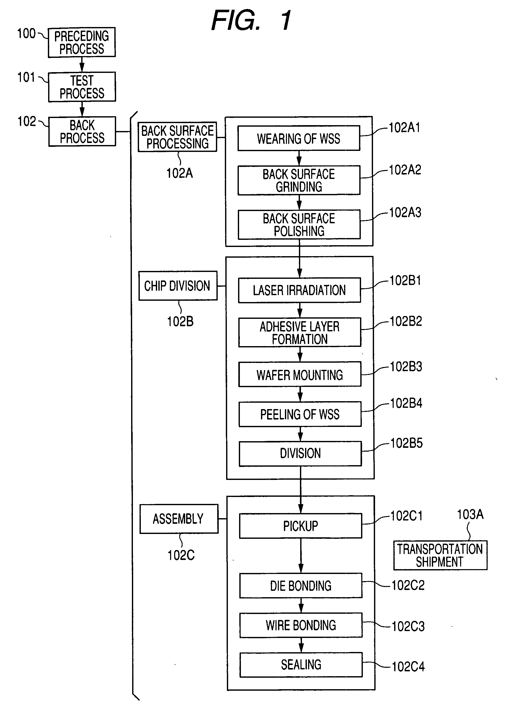
[0075] The manufacturing method of the semiconductor device of Embodiment 1 is explained along the flow diagram of FIG. 1.

[0076] First, in preceding process 100, the semiconductor wafer (henceforth a wafer) which has a main surface and a back surface which serve as the opposite side mutually along a thickness direction is prepared, and a plurality of semiconductor chips (henceforth a chip) are formed in the main surface (device formation surface) of the wafer. This preceding process 100 is also called a wafer process or a wafer fabrication, forms a chip (an element and a circuit) in the main surface of a wafer, and is a step until it changes into the state where an electrical test can be done with a probe etc. There are a film formation step, an impurity introduction (diffusion or ion implantation) step, photolithography step, an etching step, a metallizing step, a cleaning step, a test step between each step, etc. in a preceding process.

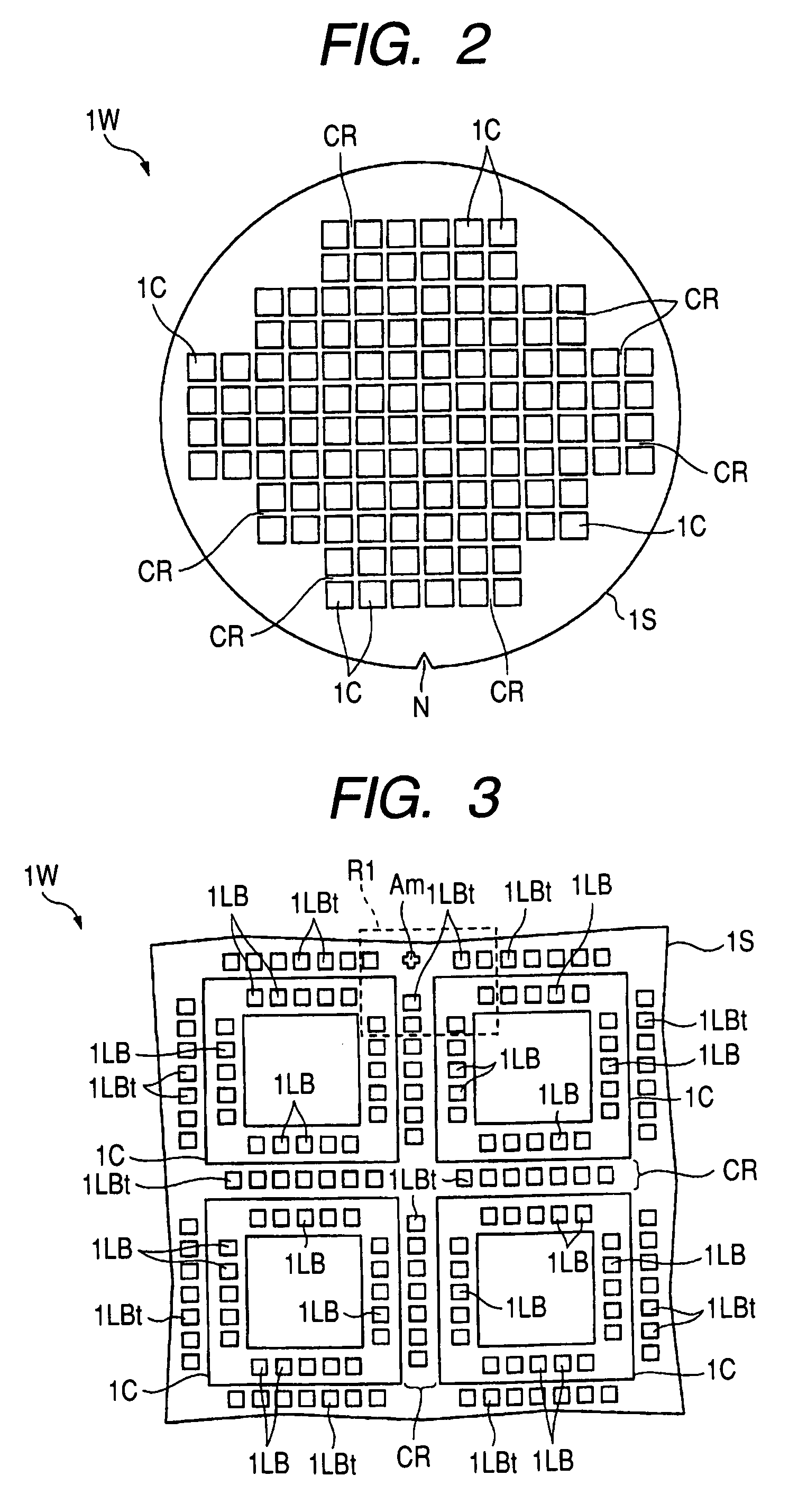
[0077]FIG. 2 shows the...

embodiment 2

[0125] (Embodiment 2)

[0126] In Embodiment 2, like the Embodiment 1, after passing through laser irradiation step 102B1 from preceding process 100 of FIG. 1, in adhesive layer forming step 102B2 of chip division step 102B, an adhesive layer is formed on the back surface of a wafer by the printing method.

[0127]FIG. 26 shows the cross-sectional view of wafer 1W at the time of the above-mentioned adhesive layer forming step 102B2, and FIG. 27 shows the plan view of mask 25A used at the time of the above-mentioned adhesive layer forming step 102B2. Although FIG. 27 was a plan view, in order to make a drawing legible, hatching was given to mask 25A.

[0128] First, on the back surface of wafer 1W, as shown in FIG. 26, after putting mask 25A where alignment is made, squeegee 26 extends binding material 8 of liquid state (paste state) along the back surface of wafer 1W from on this mask 25A. In mask 25A, as shown in FIG. 26 and FIG. 27, opening 25A1 of the almost same plane size as each chip...

embodiment 3

[0138] (Embodiment 3)

[0139] The Embodiment 1 and 2 explained the case where an adhesive layer was formed on the back surface of wafer 1W, after the laser irradiation step for forming reforming area LB in the chip division step. Embodiment 3 explains the case where the laser irradiation step for forming reforming area LB is performed in a chip division step after forming an adhesive layer on the back surface of wafer 1W.

[0140]FIG. 36 shows the flow diagram of the semiconductor device of Embodiment 3. In Embodiment 3, like the Embodiment 1, after passing through preceding process 200 and test process 201 of FIG. 36, wearing step of WSS 202A1, back surface grinding step 202A2, and back surface polishing step 202A3 of back surface processing step 202A of back process 202 are performed in order.

[0141] Then, in Embodiment 3, in chip division step 202B, before performing the laser irradiation step for forming reforming area PL, adhesive layer forming step 202B1 is performed. FIG. 37-FIG....


PUM

PropertyMeasurementUnit
Thicknessaaaaaaaaaa
Adhesion strengthaaaaaaaaaa
Areaaaaaaaaaaa

Abstract

The semiconductor device having the structure which laminated the chip in many stages is made thin. A reforming area is formed by irradiating a laser beam, where a condensing point is put together with the inside of the semiconductor substrate of a semiconductor wafer. Then, after applying the binding material of liquid state to the back surface of a semiconductor wafer by a spin coating method, this is dried and a solid-like adhesive layer is formed. Then, a semiconductor wafer is divided into each semiconductor chip by making the above-mentioned reforming area into a division origin. By pasting up this semiconductor chip on the main surface of an other semiconductor chip by the adhesive layer of the back surface, the semiconductor device having the structure for which the semiconductor chip was laminated by many stages is manufactured.

Description

CROSS-REFERENCE TO RELATED APPLICATION [0001] The present application claims priority from Japanese patent application No. 2005-231946 filed on Aug. 10, 2005, the content of which is hereby incorporated by reference into this application. FIELD OF THE INVENTION [0002] The present invention relates to the manufacturing method of a semiconductor device, and a semiconductor device technology, and particularly relates to the multi-stage layering technique of a chip. DESCRIPTION OF THE BACKGROUND ART [0003] In recent years, in connection with the size and weight reduction of the mobile computing devices represented by a cellular phone, the digital camera, etc. and the information storage medium represented by the memory card etc., densification of the semiconductor device built into these is advanced. The thickness reduction of the semiconductor chip which forms a semiconductor device is indispensable to the densification of a semiconductor device. The multi-stage laminated constitution ...

Claims


Application Information

Patent Timeline
IPC IPC(8): H01L21/58B23K26/00B23K26/364
CPCH01L21/563H01L23/3121H01L24/27H01L24/29H01L24/83H01L25/0657H01L25/50H01L2221/6834H01L2224/16225H01L2224/274H01L2224/32145H01L2224/32225H01L2224/48091H01L2224/48145H01L2224/48227H01L2224/48465H01L2224/73265H01L2224/83191H01L2224/8385H01L2224/92H01L2224/92247H01L2225/0651H01L2225/06517H01L2225/06575H01L2225/06582H01L2924/01002H01L2924/01005H01L2924/01013H01L2924/01015H01L2924/01027H01L2924/01029H01L2924/01033H01L2924/01047H01L2924/0105H01L2924/01073H01L2924/01074H01L2924/01075H01L2924/01077H01L2924/01078H01L2924/01079H01L2924/01082H01L2924/04941H01L2924/04953H01L2924/07802H01L2924/14H01L2924/15311H01L2924/0132H01L2924/0133H01L2224/73204H01L24/48H01L2224/2919H01L2924/01006H01L2924/01019H01L2924/01023H01L2924/01024H01L2924/014H01L2924/0665H01L2224/29101H01L2224/83444H01L2924/15747H01L2224/29111H01L21/82H01L2924/00014H01L2924/00012H01L2924/00H01L2924/01007H01L2924/01022H01L2924/3512H01L2224/13111H01L2924/181H01L2924/12042H01L24/73H01L2224/45144H01L24/45H01L2224/73253H01L2224/45015H01L2924/207
Inventor HIGASHINO, TOMOKOMIYAZAKI, CHUICHIABE, YOSHIYUKI
Owner RENESAS ELECTRONICS CORP
Why Eureka
Try Eureka