
Source/drain electrodes, thin-film transistor substrates, manufacture methods thereof, and display devices

a technology of source/drain electrode and substrate, which is applied in the direction of semiconductor devices, semiconductor/solid-state device details, electrical apparatus, etc., can solve the problems of decreased switching speed of thin-film transistor, increased leak current flowing, and reduced on-state current, so as to achieve excellent productivity, good thin-film transistor properties, and excellent thin-film transistor properties.

Active Publication Date: 2007-02-22
KOBE STEEL LTD
View PDF13 Cites 55 Cited by
  • Summary
  • Abstract
  • Description
  • Claims
  • Application Information

AI Technical Summary

Benefits of technology

[0030] The present invention has been accomplished under these circumstances, and an object of the present invention is to provide a technique that gives excellent thin-film transistor properties even without lower barrier metal layer and permits direct and reliable connection between source / drain interconnections and semiconductor layers of thin-film transistors.
[0031] Another object of the present invention is to provide a technique that ensures excellent thin-film transistor properties, high thermal stability, and low contact resistivity without lower and upper barrier metal layers and permits direct and reliable connection of source / drain interconnections not only to semiconductor layers of thin-film transistors but also to transparent picture electrodes.
[0064] The source / drain electrodes according to the present invention have the above configuration, can use a generally used pure aluminum or aluminum alloy. In addition, they can be connected to semiconductor layers of thin-film transistors through the nitrogen-containing layer without barrier metal layers, in contrast to conventional equivalents. The source / drain electrodes have good thin-film transistor properties.
[0065] By further using an Al—Ni alloy containing a specific amount of nickel as the aluminum alloy, the source / drain electrodes according to the present invention can be directly connected not only to semiconductor layers of thin-film transistors but also to transparent picture electrodes. The resulting source / drain electrodes are excellent in thin-film transistor properties, contact resistivity, and thermal stability.
[0066] The use of the source / drain electrodes according to the present invention provides high-performance display devices that can be produced with excellent productivity at low cost.

Problems solved by technology

Consequently, the performance of the amorphous silicon as a semiconductor significantly deteriorates, resulting in a decreased ON-state current, an increased leak current flowing when the thin-film transistor is turned off (OFF-state current), and / or a decreased switching speed of the thin-film transistor.
Thus, desired thin-film transistor properties cannot be obtained, and the resulting display device has poor performance and quality.
The system including extra units for the deposition of barrier metal layers causes an increased production cost and a reduced productivity, which must be avoided in mass-production of liquid crystal panels at low cost.
If an aluminum alloy thin film is directly connected to the transparent picture electrode, the contact resistance between these components is high, which impairs the quality of displayed images.
Aluminum used as a material for the interconnections for the transparent picture electrode is very susceptible to oxidation.
The indium tin oxide (ITO) as a material for the transparent picture electrode is an electrically conductive metal oxide, but it fails to establish an electrically Ohmic contact if an aluminum oxide layer is formed as mentioned above.
These extra units cause an increased production cost and a decreased productivity.
Thus, processing dimensions in transverse or crosswise direction in the processing cannot be significantly controlled.
Accordingly, the deposition of barrier metal layers requires complicated processes and thereby causes an increased production cost and a decreased productivity, not only from the viewpoint of film-deposition but also from the viewpoint of processing.
According to this technique, however, the ITO film that is most widely used must be replaced with the IZO film, which causes an increased material cost.
The method, however, requires an extra step for the surface treatment, which causes a decreased productivity.
This method, however, requires an extra step of depositing the second layer containing impurities.
To avoid this problem, the method requires frequent maintenance operations while stopping the film-deposition step, and this results in a significantly decreased productivity.
In addition, the method is still susceptible to improvements in contact resistance and Ohmic contact, and a demand has been made on further improvements.
The above explanation has been made by taking a liquid crystal display device as a representative example, but the problems in the conventional techniques are in common in amorphous silicon thin-film transistor substrates used not only in liquid crystal display devices but also in other devices.
These problems also occur in thin-film transistor substrates using a polycrystalline silicon instead of an amorphous silicon as the semiconductor layer of thin-film transistors.

Method used


Image

  • Source/drain electrodes, thin-film transistor substrates, manufacture methods thereof, and display devices
  • Source/drain electrodes, thin-film transistor substrates, manufacture methods thereof, and display devices
  • Source/drain electrodes, thin-film transistor substrates, manufacture methods thereof, and display devices

Examples


experimental examples

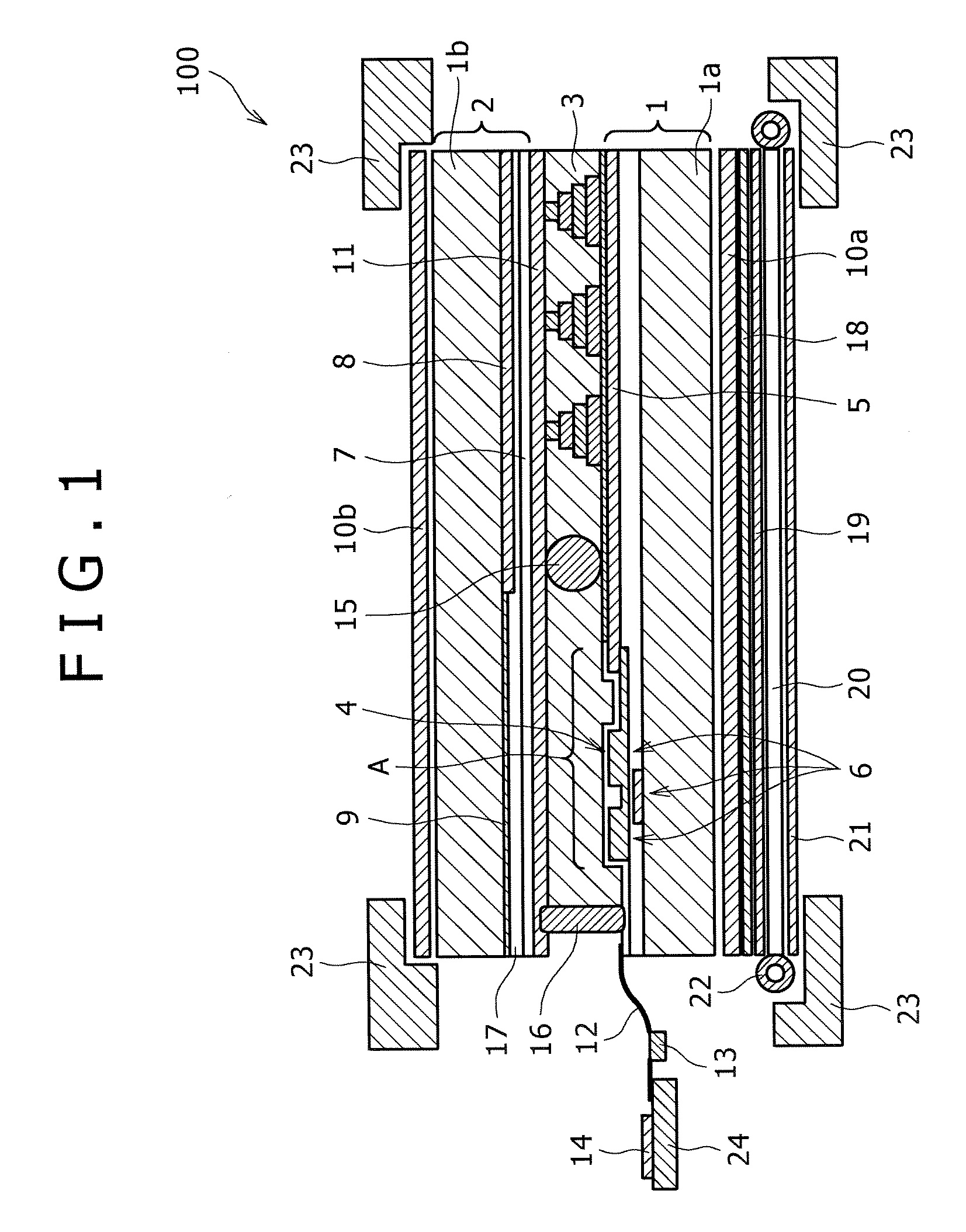
[0170] Experiments were conducted in following Experimental Examples 1 to 5 to verify that excellent thin-film transistor properties can be obtained even without barrier metal layers by using source / drain electrodes containing a nitrogen-containing layer as in the present invention. The experimental conditions and determination methods of the properties are as follows.

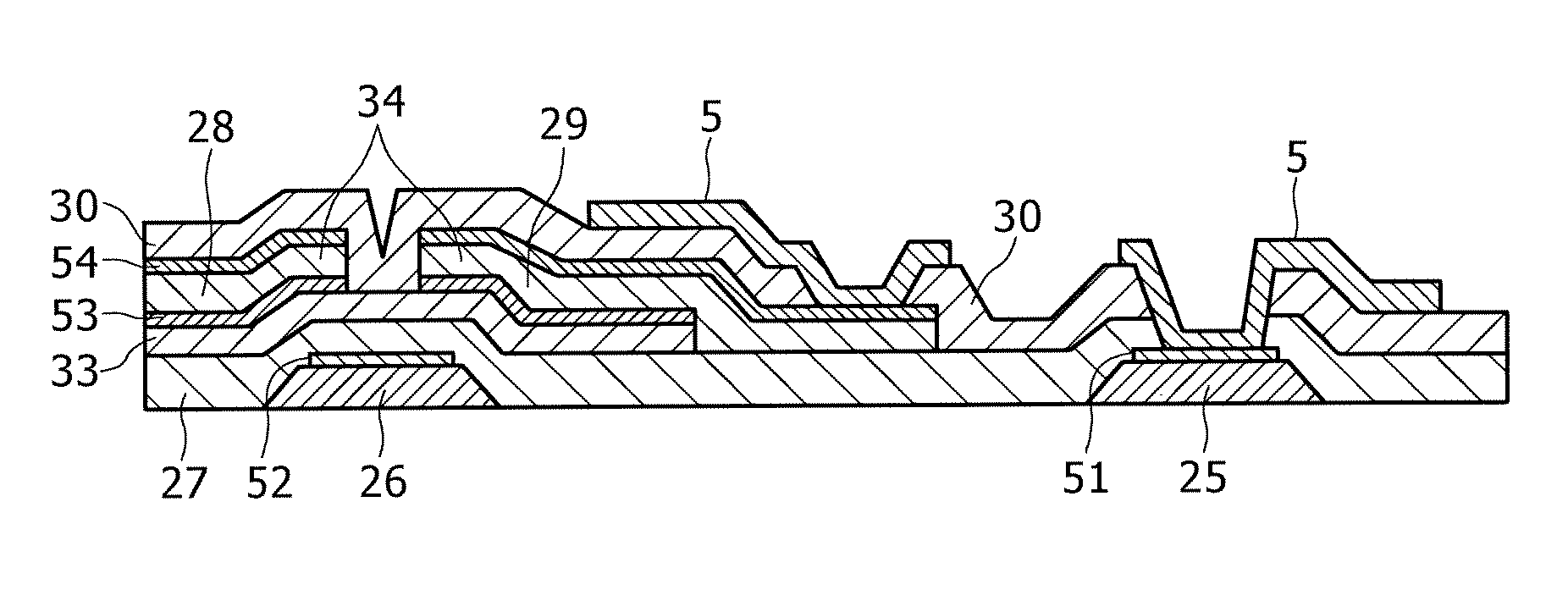
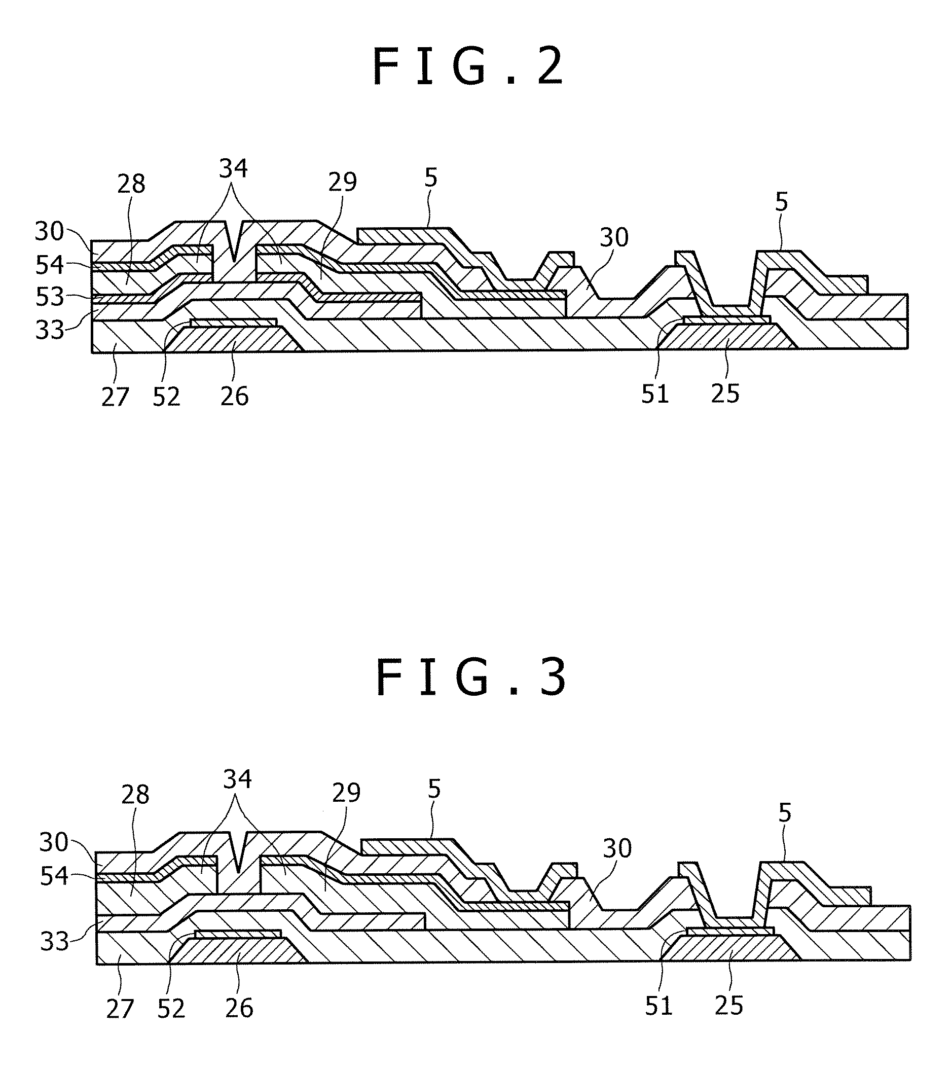
[0171] Source / drain Electrodes

[0172] The source / drain electrodes according to Embodiment 1 using Al-2.0 atomic percent Ni alloy were used in Experimental Examples 1 to 4. The source / drain electrodes according to Embodiment 1 were used in Experimental Example 5, except for using pure aluminum instead of the Al-2.0 atomic percent Ni alloy. Experimental Examples 1 to 4 differ from one another only by the formation method of the nitrogen-containing layer for the source / drain electrodes. Specifically, the nitrogen-containing layer was formed by the plasma nitridation process in Experimental Example 1, which process is des...

experimental example 1

[0173] A thin-film transistor was prepared by the procedure of Embodiment 1.

experimental example 2

[0174] A thin-film transistor was prepared by the procedure of Embodiment 1, except for forming a nitrogen-containing layer in the following manner.

[0175] Initially, an n+-type hydrogenated amorphous silicon film (n+a-Si—H) 56 was formed by the procedure of Embodiment 1. Next, heating was conducted using nitrogen gas as a carrier gas at 350° C. for thirty minutes in the plasma nitridation system used for the deposition of the silicon nitride film. The surface of the work after heating was analyzed by the procedure of Embodiment 1 to find that a nitrogen-containing layer was formed to a thickness of about 6 nm.


PUM


Abstract

A source / drain electrode is used in a thin-film transistor substrate containing a substrate, a thin-film transistor semiconductor layer, source / drain electrodes, and a transparent picture electrode. The source / drain electrode includes a nitrogen-containing layer and a thin film of pure aluminum or an aluminum alloy. Nitrogen of the nitrogen-containing layer binds to silicon of the thin-film transistor semiconductor layer, and the thin film of pure aluminum or aluminum alloy is connected to the thin-film transistor semiconductor layer through the nitrogen-containing layer.

Description

BACKGROUND OF THE INVENTION [0001] 1. Field of the Invention [0002] The present invention relates to source / drain electrodes and substrates for use in thin-film transistors of liquid crystal displays, semiconductor devices, and optical components. It also relates to methods for manufacturing the substrates, and display devices. Specifically, it relates to novel source / drain electrodes containing a thin film of pure aluminum or aluminum alloy as a component. [0003] 2. Description of the Related Art [0004] Liquid crystal display devices are used in a variety of applications ranging from small-sized mobile phones to large-sized television sets with 30-inch or larger screens. They are categorized by the pixel driving method into simple-matrix liquid crystal display devices and active-matrix liquid crystal display devices. Of these, active-matrix liquid crystal display devices having a thin-film transistor (hereinafter briefly referred to as TFT) as a switching element are widely used, b...

Claims


Application Information

Patent Timeline
IPC IPC(8): H01L29/04
CPCH01L29/458H01L29/4908H01L29/66765H01L27/124
Inventor KAWAKAMI, NOBUYUKIKUGIMIYA, TOSHIHIROGOTOH, HIROSHITOMIHISA, KATSUFUMIHINO, AYA
Owner KOBE STEEL LTD
Learn More