System and method for injecting phase jitter into integrated circuit test signals

a technology of integrated circuit and phase jitter, which is applied in the field of system and method for injecting phase jitter into integrated circuit test signals, can solve the problems of rapid change in timing, more difficult for digital signals to be acquired or captured by a receiving device during the eye, and the random variation of the switching time of a digital circui

Inactive Publication Date: 2007-02-22
MICRON TECH INC
View PDF24 Cites 15 Cited by
  • Summary
  • Abstract
  • Description
  • Claims
  • Application Information

AI Technical Summary

Problems solved by technology

For example, the period for which a digital signal is valid, known as the “eye,” decreases as the data rate increases, thereby making it more difficult for the digital signal to be acquired or captured by a receiving device during the eye.
One factor affecting the location of the data eye is “phase jitter,” which is high frequency phase noise that causes rapid changes in the timing at which transitions of digital signals occur.
Phase jitter can be caused by a number of sources, such as noise coupled to digital circuits, which causes the switching time of a digital circuit to vary in a random manner.
Jitter can also be caused by variations in the propagation time of digital signals coupled through signal lines.
The location of the data eye can also be affected by timing skew, duty cycle variation, and other types of unwanted signal distortion.
Similar problems exist in coupling other signals, such as command and address signals, to the memory device, as well as coupling read data signals and a read strobe signal from the memory device and coupling digital signals to other devices.
However, normal jitter is neither regular nor periodic.
Therefore, conventional testing systems and methods for injecting jitter in digital test signals do not accurately simulate the jitter that will be present in signals during normal operation.

Method used


Image

  • System and method for injecting phase jitter into integrated circuit test signals
  • System and method for injecting phase jitter into integrated circuit test signals
  • System and method for injecting phase jitter into integrated circuit test signals

Examples


Embodiment Construction

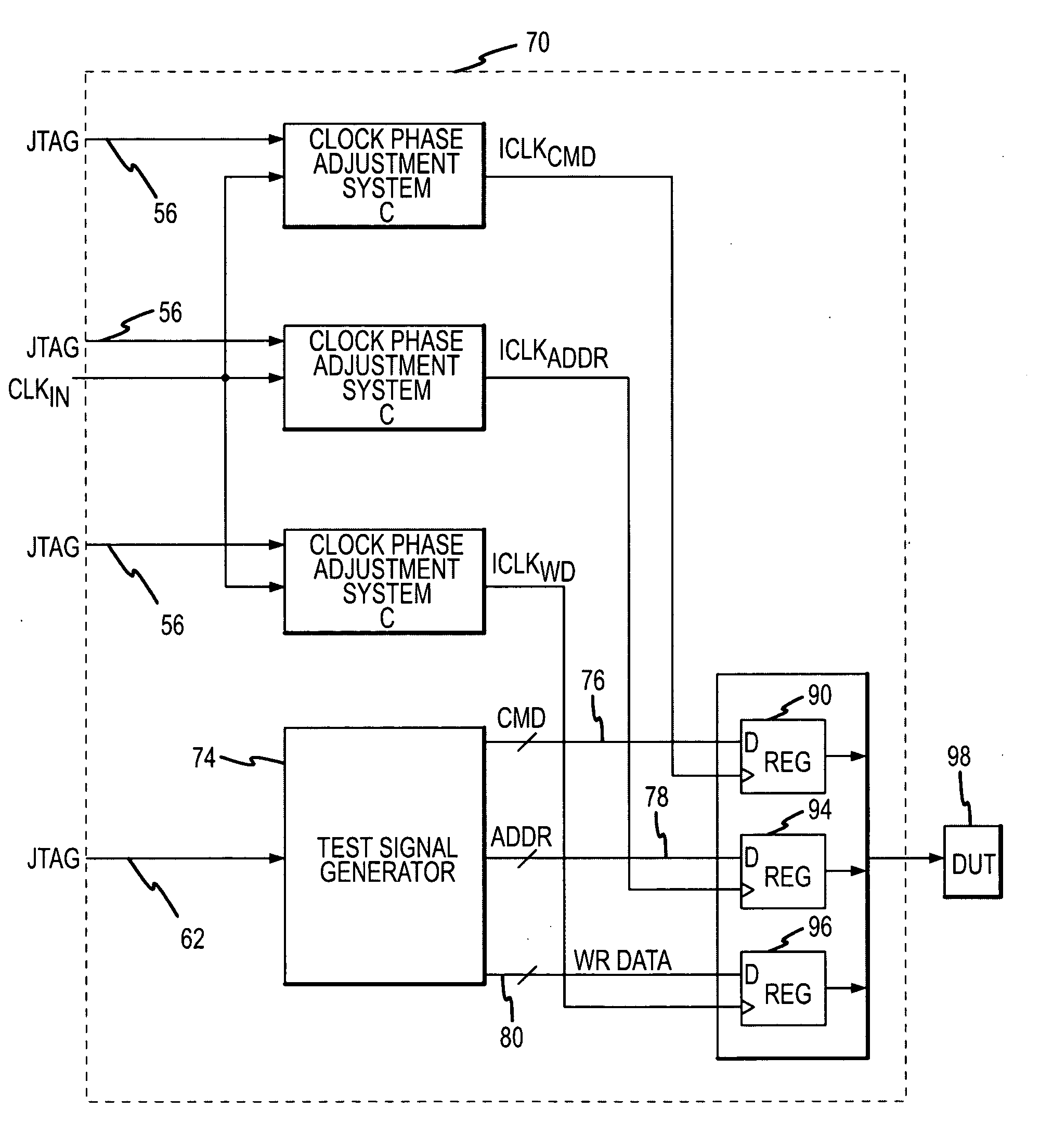
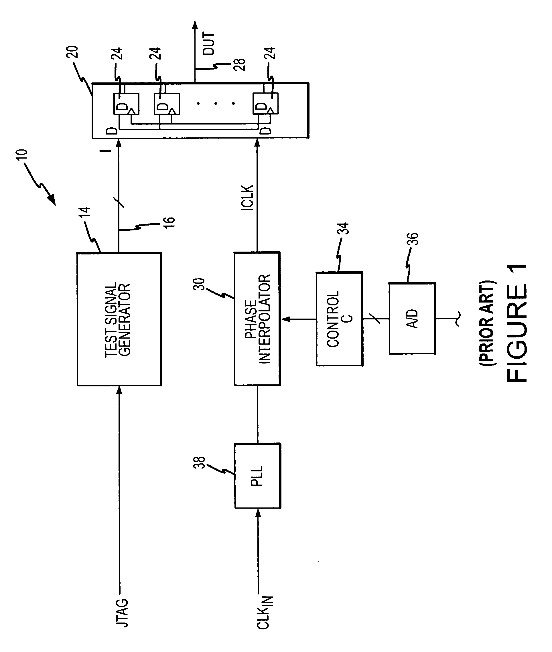
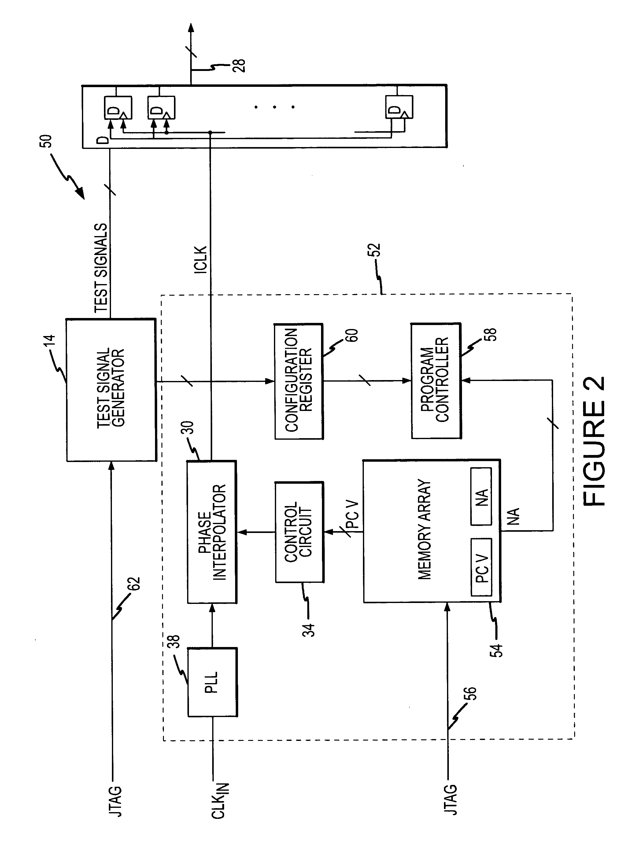
[0018] A test system 50 according to one example of the present invention is shown in FIG. 2. The test system 50 includes a clock phase adjustment system 52 that uses some of the same components that are used in the prior art test system 10 of FIG. 1. Therefore, in the interest of brevity, an explanation of their operation will not be repeated. The test system 50 differs from the test system 10 shown in FIG. 1 in the manner in which the clock jitter system generates the phase control values that are applied to the control input of the control circuit 34. More specifically, in the test system 50, the phase control values are read from a memory array 54 at a location corresponding to an address from a program controller 58.

[0019] As shown in FIG. 2, the memory array 54 includes two fields at each address, namely the phase control value (“PCV”) field and a next address word (“NA”) field. The memory array 54 may be programmed with the phase control value and next address word pairs thr...


PUM


Abstract

A memory test system injects phase jitter in memory command, address and write data signals in respective pin groups. A phase interpolator receiving a clock signal is provided for each of the pin groups to generate respective delayed clock signals. The phase shift produced by each of the phase interpolators is determined by delay control values, which are passed to the phase interpolators from respective memory arrays. Each of the memory arrays stores at each address a next address along with a delay control value. The next address is used to access the memory array to obtain next delay control value. The delayed clock signals are applied to a clock input of a respective set of registers for each pin group, and a data input of each of the registers receives one of the memory device signals in the respective pin group.

Description

TECHNICAL FIELD [0001] This invention relates to testing integrated circuit devices, and, more particularly, to testing integrated circuits in the presence of phase jitter in a manner that causes the signals to have phase jitter of the type that is likely to occur in an operating environment. BACKGROUND OF THE INVENTION [0002] As the operating speeds of integrated circuits such as memory devices continues to increase, the timing margins for test signals applied to and received from the integrated circuits continues to decrease. For example, the period for which a digital signal is valid, known as the “eye,” decreases as the data rate increases, thereby making it more difficult for the digital signal to be acquired or captured by a receiving device during the eye. In memory systems, write data signals are normally transmitted to a memory device along with a write data strobe signal. The timing of the write data strobe signal is selected so that a transition of the write data strobe s...

Claims


Application Information

Patent Timeline
Patent Type & Authority Applications(United States)
IPC IPC(8): G11C7/00
CPCG11C7/22G11C7/222G11C29/50G11C29/50012G11C29/56G11C29/56012
Inventor JEDDELOH, JOSEPH M.
Owner MICRON TECH INC
Why Eureka
Try Eureka