Method for fabricating semiconductor device

a semiconductor and device technology, applied in semiconductor/solid-state device manufacturing, basic electric elements, electric devices, etc., can solve the problems of obstructing affecting the yield of the device, and affecting the development of multi-layer interconnection, so as to facilitate the the effect of unacceptable delamination from the edg

Inactive Publication Date: 2007-02-22
PANASONIC CORP
View PDF1 Cites 17 Cited by
  • Summary
  • Abstract
  • Description
  • Claims
  • Application Information

AI Technical Summary

Benefits of technology

[0010] When the interconnect layer is formed by the above process steps, however, delamination from the edge of the wafer occurs to affect the yield of the device. The term “the edge of a wafer (or a wafer edge)” in this description means a region of a wafer located outside a chip formation region (semiconductor element formation region), while the term “a bevel (or a wafer bevel)” means a portion of a wafer contained in the wafer edge and having the surface inclined relative to the plane of the chip formation region. Following wafer size enlargement, the ratio of the number of chips on the wafer outer region to the total number of chips on the wafer increases, so that delamination from the edge becomes unacceptable. In addition, as the number of interconnect layers increases, delamination from the edge is facilitated. This obstructs development of multi-layer interconnection.

Problems solved by technology

When the interconnect layer is formed by the above process steps, however, delamination from the edge of the wafer occurs to affect the yield of the device.
Following wafer size enlargement, the ratio of the number of chips on the wafer outer region to the total number of chips on the wafer increases, so that delamination from the edge becomes unacceptable.
This obstructs development of multi-layer interconnection.

Method used


Image

  • Method for fabricating semiconductor device
  • Method for fabricating semiconductor device
  • Method for fabricating semiconductor device

Examples


first embodiment

[0029] A method for fabricating a semiconductor device according to a first embodiment of the present invention will be described below with reference to the accompanying drawings.

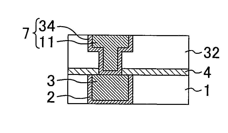
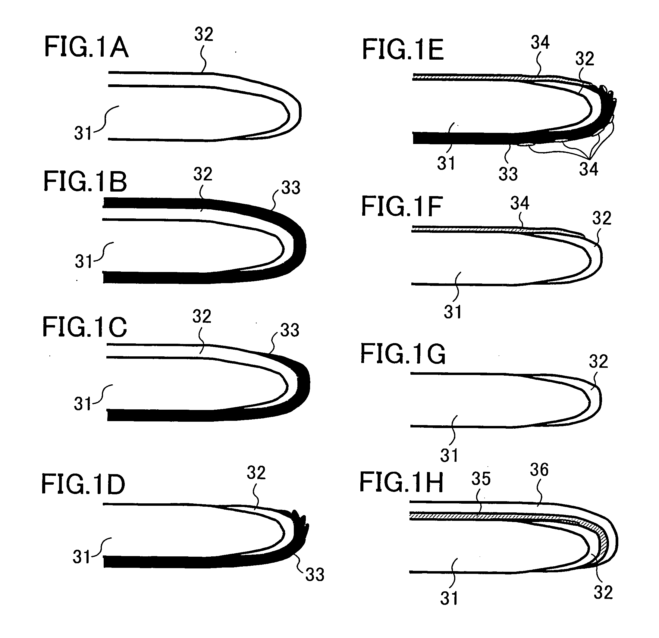
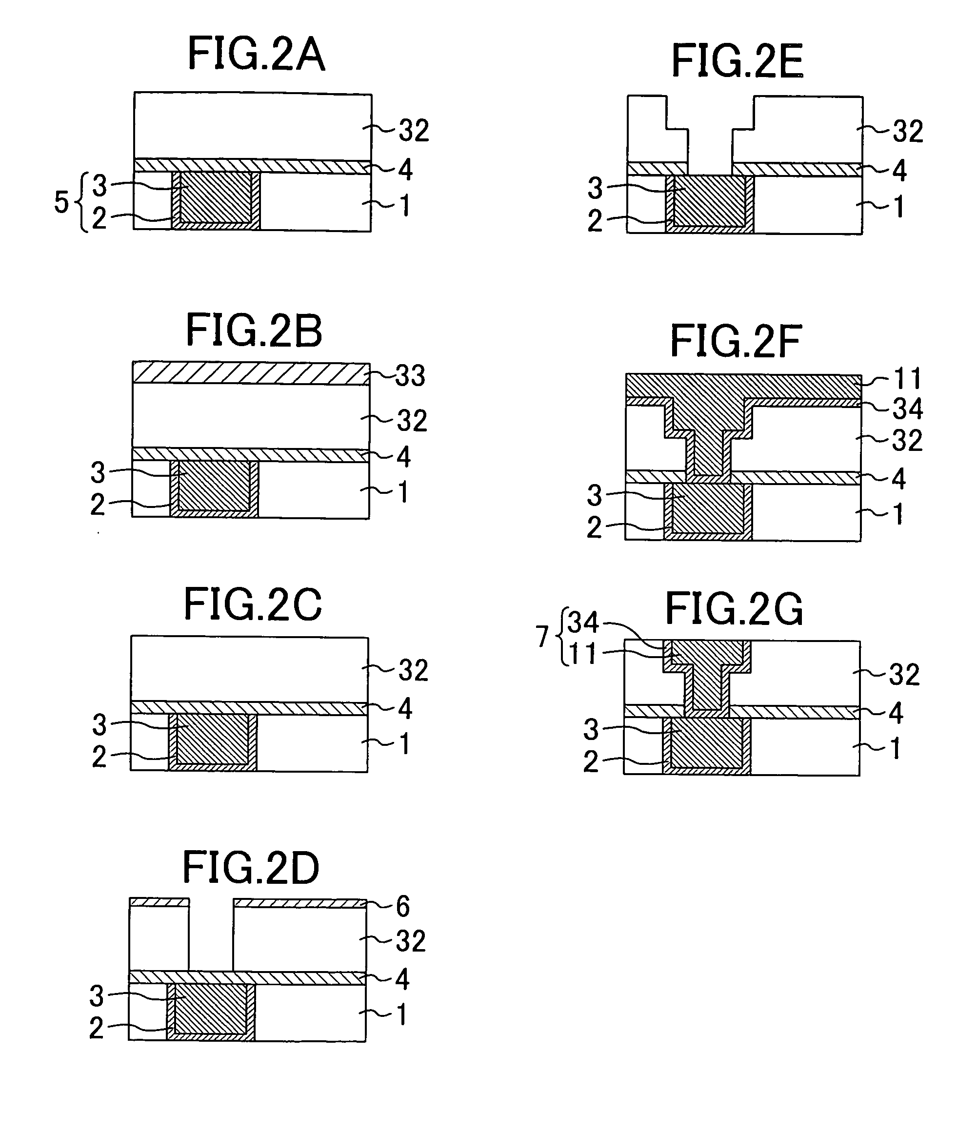
[0030]FIGS. 1A to 1H are sectional views of a wafer edge for explaining the method for fabricating a semiconductor device according to the first embodiment. FIGS. 2A to 2G are sectional views of a chip formation region of the wafer for explaining the method for fabricating a semiconductor device according to the first embodiment.

[0031] Referring to FIG. 1A, first, an organic-based low-dielectric-constant interlayer film (referred hereinafter to as an organic-based low-k interlayer film) 32 made of SiOC or the like is formed over the top surface of a wafer-shaped semiconductor substrate 31. During this formation, the organic-based low-k interlayer film 32 is formed also on the edge of the semiconductor substrate 31 including the bevel. As shown in FIG. 2A, in a chip formation region on the principal surfa...

second embodiment

[0043] A method for fabricating a semiconductor device according to a second embodiment of the present invention will be described below with reference to the accompanying drawings. The method of the second embodiment simplifies fabrication steps as compared to that of the first embodiment by modifying the step of depositing a protective film and the step of removing a portion of the protective film on a device surface.

[0044]FIGS. 3A to 3H are sectional views for explaining the method for fabricating a semiconductor device according to the second embodiment. These figures illustrate an edge of a wafer-shaped semiconductor substrate.

[0045] As shown in FIG. 3A, first, in the edge of a wafer-shaped semiconductor substrate 41, an organic-based low-k interlayer film 42 is formed on the semiconductor substrate 41. Unlike the first embodiment, the organic-based low-k interlayer film 42 is not polished in this step.

[0046] Next, as shown in FIG. 3B, using a thermal CVD method, a protectiv...


PUM


Abstract

In a Cu interconnect process, an organic-based low-dielectric-constant interlayer film is formed, and then a protective film is deposited on the side and back surfaces of a wafer bevel and the back surface of a wafer edge. Thereafter, a lithography process and an etching process are carried out, a copper film is formed, and then the protective film is removed.

Description

BACKGROUND OF THE INVENTION [0001] (a) Fields of the Invention [0002] The present invention relates to methods for fabricating a semiconductor device, and in particular to interconnect formation processes using an insulating-layer formation material and a metal material serving as an interconnect layer. [0003] (b) Description of Related Art [0004] With shrinking design rules of semiconductor devices, circuit integration in the devices dramatically increases, so that more than one hundred million transistors can be provided on one chip. To provide such a chip, not only microfabrication technologies such as lithography and etching are developed which require a processing accuracy of the order of several tens of nanometers, but also lowered resistance of interconnects, lowered dielectric constant of interlayer insulating films, and multi-layer interconnection are needed. [0005] A method for forming an interconnect of a semiconductor device using a low dielectric constant insulating mat...

Claims


Application Information

Patent Timeline
Patent Type & Authority Applications(United States)
IPC IPC(8): H01L21/4763
CPCH01L21/768H01L21/76807
Inventor TAKEOKA, SHINJI
Owner PANASONIC CORP
Why Eureka
Try Eureka