

Wafer drilling method
a drilling method and a technology of a wafer, applied in the direction of welding/soldering/cutting articles, manufacturing tools, semiconductor/solid-state device details, etc., can solve the problem that the productivity of the drilling process is not always satisfactory, and achieve the effect of efficient drilling
- Summary
- Abstract
- Description
- Claims
- Application Information
AI Technical Summary
Benefits of technology
Problems solved by technology
Method used
Image

Examples
first embodiment
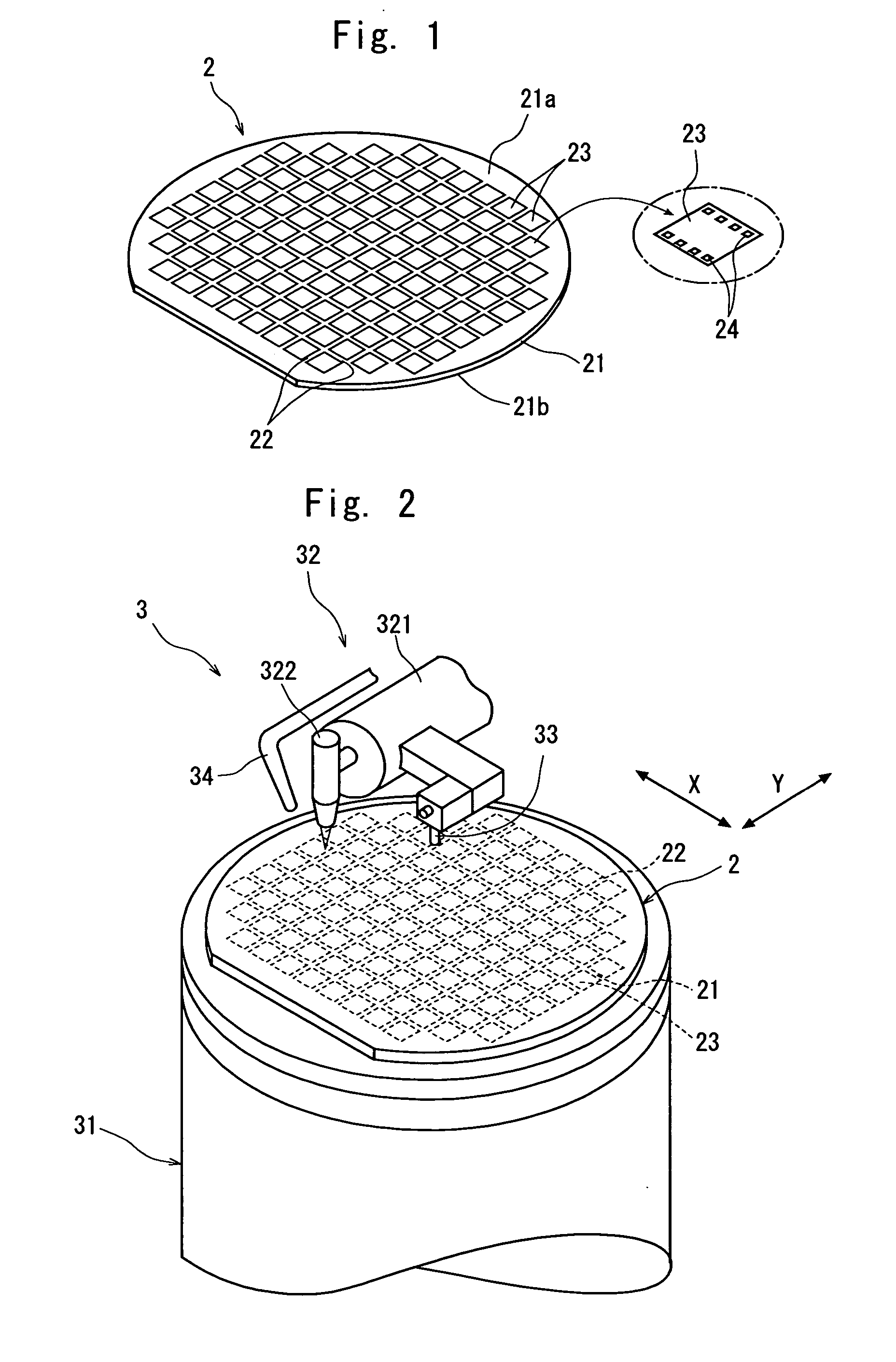
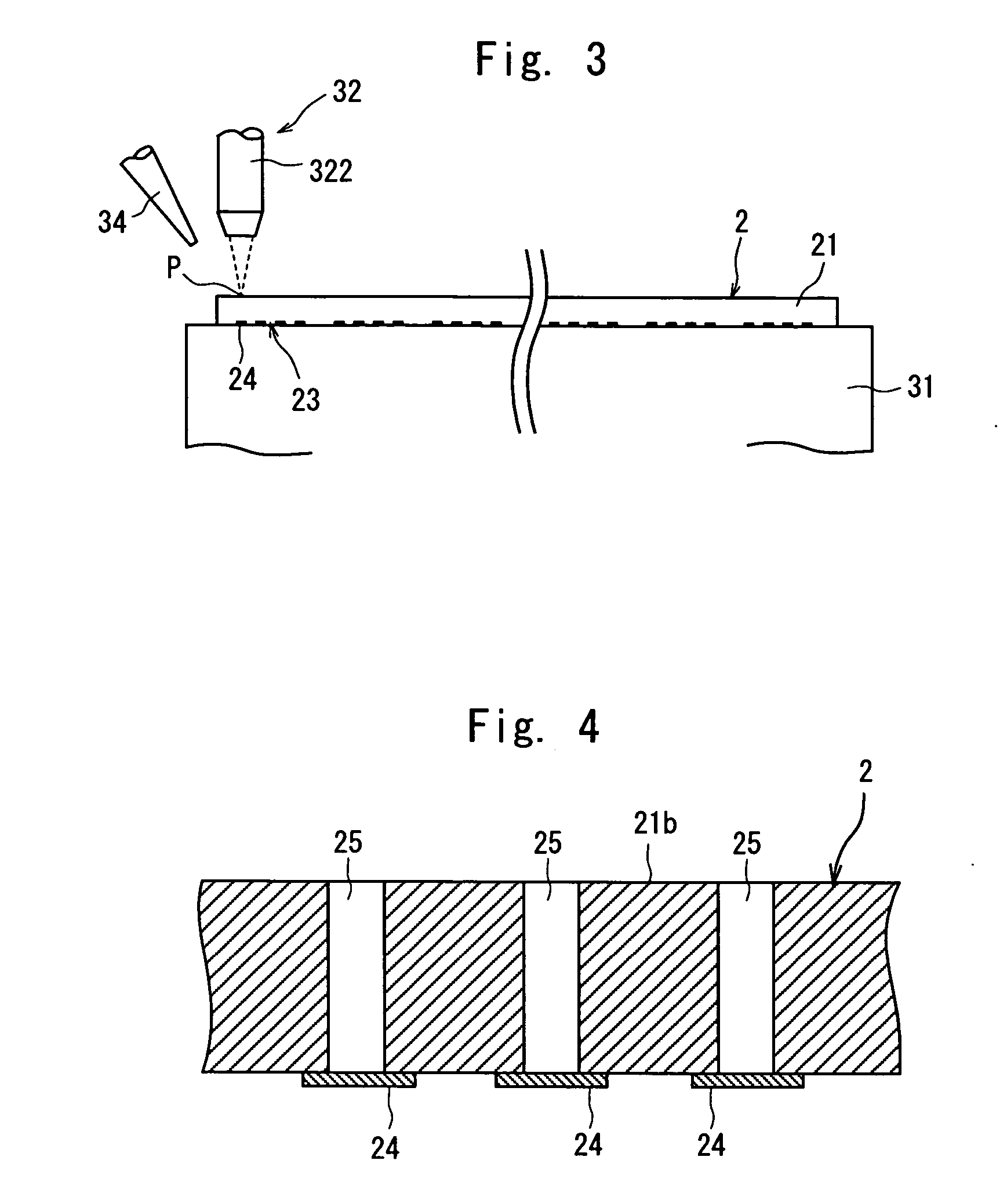
[0030] A description will be first given of the laser beam application step.
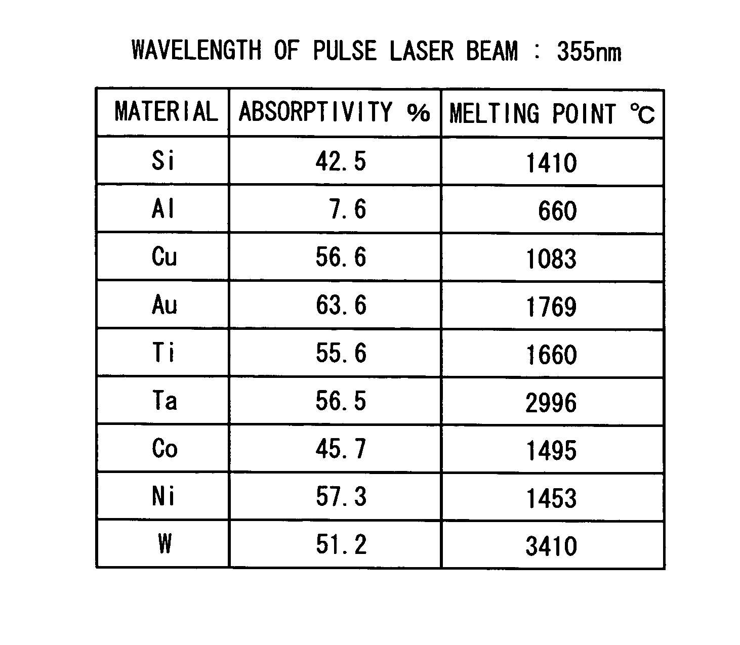
[0031] In the first embodiment, the material forming the substrate 21, the material forming the electrodes 24 and the wavelength of the pulse laser beam are selected based on absorptivity for the wavelength of the pulse laser beam. That is, the material forming the substrate 21, the material forming the electrodes 24 and the wavelength of the pulse laser beam are set to ensure that the absorptivity of the electrodes 24 for the wavelength of the pulse laser beam should become lower than that of the substrate 21 for the wavelength of the pulse laser beam. More specifically, in this embodiment, the substrate 21 of the semiconductor wafer 2 is made of silicon, the electrodes 24 are made of aluminum, and the wavelength of the pulse laser beam applied from the condenser is set to 355 nm.
[0032] That is, after the electrode 24 at the most left end out of the plurality of electrodes 24 formed on the device 23 at the...
second embodiment
[0044] A description will be subsequently given of the laser beam application step.
[0045] In the second embodiment, the material forming the substrate 21, the material forming the electrodes 24 and the wavelength of the pulse laser beam are selected based on the melting points of the materials forming the substrate 21 and the electrodes 24 and absorptivity for the wavelength of the pulse laser beam. That is, the material forming the substrate 21, the material forming the electrodes 24 and the wavelength of the pulse laser beam are set to ensure that the substrate 21 reaches its melting point but the electrodes 24 do not reach their melting point. More specifically, in this embodiment, the substrate 21 of the semiconductor wafer 2 is made of silicon, the electrodes 24 are made of gold (Au), titanium (Ti), tantalum (Ta) or tungsten (W), and the wavelength of the pulse laser beam applied from the condenser is set to 532 nm.
[0046]FIG. 6 shows the absorptivities for a pulse laser beam h...
PUM
| Property | Measurement | Unit |
|---|---|---|
| Nanoscale particle size | aaaaa | aaaaa |
| Wavelength | aaaaa | aaaaa |
| Melting point | aaaaa | aaaaa |
Abstract
Description
Claims
Application Information