Method and fabricating semiconductor memory device

a memory device and semiconductor technology, applied in semiconductor devices, semiconductor/solid-state device details, thin material processing, etc., can solve the problems of low operation voltage and general limitations of the typical method, and achieve the effect of improving operation characteristics and decreasing bit line resistan

Inactive Publication Date: 2007-03-01
SK HYNIX INC
View PDF8 Cites 11 Cited by
  • Summary
  • Abstract
  • Description
  • Claims
  • Application Information

AI Technical Summary

Benefits of technology

[0009] Consistent with the present invention, a method for fabricating a semiconductor memory device is provided, which can improve an operation characteristic by decreasing a bit line resistance.

Problems solved by technology

High speed and low power consuming operations are generally demanded in recent DRAMs, and consequently, a low operation voltage is demanded.
Limitations of the typical method are generally occurred when using the diffusion barrier metal layer including the titanium nitride / titanium layer between a tungsten layer and silicon.

Method used


Image

  • Method and fabricating semiconductor memory device
  • Method and fabricating semiconductor memory device
  • Method and fabricating semiconductor memory device

Examples


Embodiment Construction

[0020] A method for fabricating a semiconductor memory device consistent with embodiments of the present invention will be described in detail with reference to the accompanying drawings. Furthermore, identical reference numerals through out the exemplary embodiments of the present invention represent identical or like elements in different drawings.

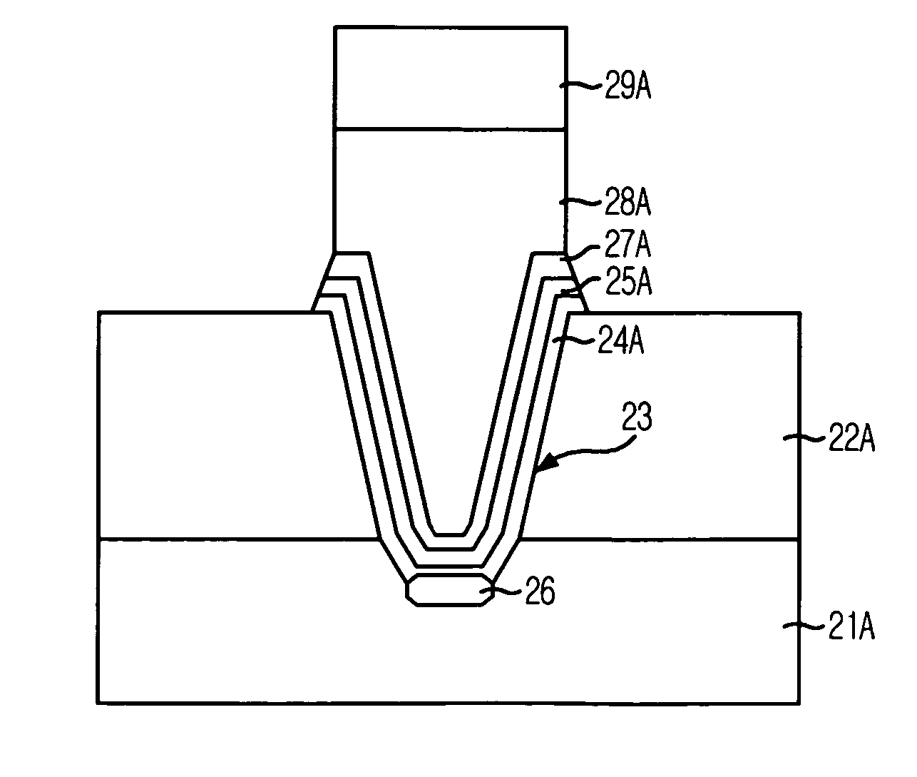
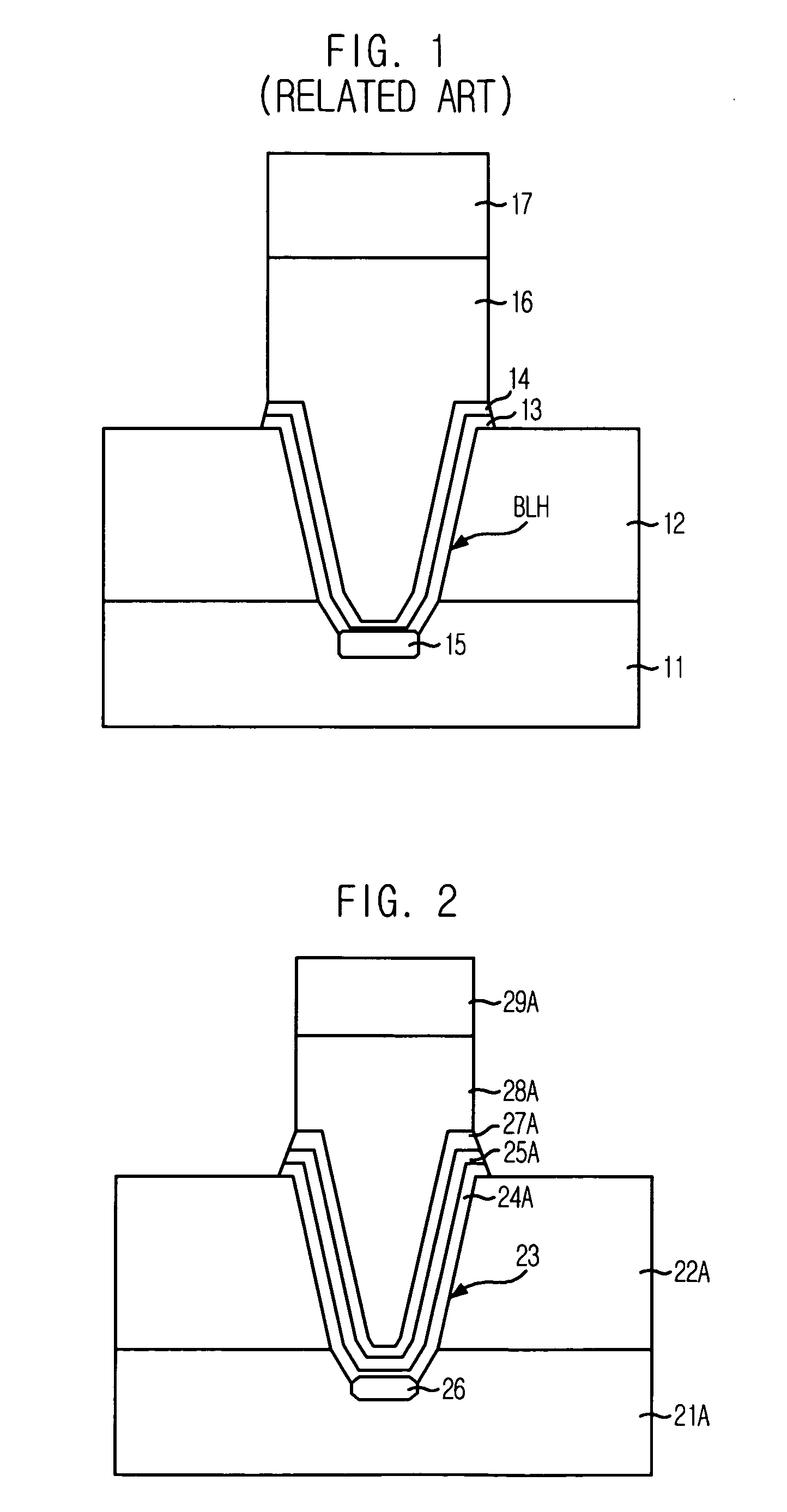
[0021]FIG. 2 illustrates a cross-sectional view of a semiconductor memory device consistent with an embodiment of the present invention. A patterned titanium layer 24A, a patterned titanium nitride layer 25A, and a patterned thin layer 27A are formed over a patterned substrate 21A. Patterned thin layer 27A is formed to increase a grain size of a subsequently formed metal layer, which may be, for example, a patterned bit line tungsten layer 28A. Patterned bit line tungsten layer 28A and a bit line hard mask 29A are formed over patterned thin layer 27A.

[0022] Patterned thin layer 27A includes tungsten silicide and has a thickness ranging...


PUM

PropertyMeasurementUnit
temperatureaaaaaaaaaa
grain sizeaaaaaaaaaa

Abstract

A semiconductor memory device includes a titanium layer and a titanium nitride layer formed on a substrate, a thin layer formed on the titanium nitride layer, and a metal layer formed on the thin layer, wherein the thin layer increases a grain size of the metal layer.

Description

RELATED APPLICATION [0001] This application is based upon and claims the benefit of priority to Korean Application No. 10-2005-0079535, filed on Aug. 29, 2005, the entire contents of which are incorporated herein by reference. TECHNICAL FIELD [0002] The present invention relates to a method for fabricating a semiconductor device, and more particularly, to a method for forming a barrier metal layer of a bit line in a semiconductor memory device. DESCRIPTION OF RELATED ARTS [0003] Tungsten (W) has been used instead of tungsten silicide (WSix) to decrease a resistance of a bit line in a typical memory device such as a dynamic random access memory (DRAM). A tungsten bit line may typically utilize a double layer including a titanium nitride layer and a titanium layer as a diffusion barrier metal layer. The double layer may include TiN / Ti or TiN / TiSix. Employing the diffusion barrier metal layer may reduce the mutual diffusion of tungsten or silicon at a region contacting a substrate, i.e...

Claims


Application Information

Patent Timeline
Patent Type & Authority Applications(United States)
IPC IPC(8): H01L23/48
CPCH01L21/76846Y10T428/265H01L27/10885Y10T428/31678H10B12/482H10B12/00
Inventor LIM, KWAN-YONGSUNG, MIN-GYUCHO, HEUNG-JAE
Owner SK HYNIX INC
Why Eureka
Try Eureka