Semiconductor constructions and methods of forming layers

a technology of semiconductors and construction methods, applied in the direction of superimposed coating process, liquid/solution decomposition chemical coating, resistive material coating, etc., can solve the problems of difficult in practice to form a conformal layer across a complex topography using coating type methods

Active Publication Date: 2007-03-01
MICRON TECH INC
View PDF5 Cites 39 Cited by
  • Summary
  • Abstract
  • Description
  • Claims
  • Application Information

AI Technical Summary

Benefits of technology

[0009] In one aspect, the invention includes a method of forming a layer. A material is provided which has at least one opening extending therein. A surface of the material is exposed to one or more of titanium oxide, neodymium oxide, yttrium oxide, zirconium oxide and vanadium oxide to activate said surface. The activated surface extends into the opening. The activated surface is exposed to a component, and such component is incorporated into a layer that extends conformally along the activated surface and into the opening.
[0010] In one aspect, the invention includes a method of forming an aluminum-containing layer. A semiconductor substrate is provided which has an insulative material thereover. The insulative material has an undulating outer surface that extends into one or more openings. The undulating surface of the insulative material is treated with one or more oxides selected from the group consisting of titanium oxide, neodymium oxide, yttrium oxide, zirconium oxide and vanadium oxide. The treated surface is exposed to one or both of aluminum silane, and aluminum silazane to form an aluminum-containing layer that extends conformally along the treated undulating surface.
[0011] In one aspect, the invention includes a semiconductor construction. The construction comprises a semiconductor substrate having an electrically insulative material thereover. The electrically insulative material has one or more openings extending therein, and has an undulating outer surface extending into the one or more openings. A liner is along the undulating outer surface. The liner is conformal with the outer surface and comprises one or more oxides selected from the group consisting of titanium oxide, neodymium oxide, yttrium oxide, zirconium oxide and vanadium oxide. The construction further includes a layer over the liner and directly against the liner. The layer extends conformally along the liner and comprises one or more of aluminum, copper, gallium, germanium, ruthenium and silicon.
[0012] In one aspect, the invention includes an electronic system. Such system includes a semiconductor substrate and an electrical node supported by the substrate. The system also includes an electrically insulative material over the substrate and having an opening extending therethrough to the electrical node. The insulative material has an undulating outer surface that extends into the opening as a sidewall periphery of the opening. The system also includes circuitry over the insulative material, and a liner along the undulating outer surface. The liner is conformal with the outer surface and comprises one or more oxides selected from the group consisting of titanium oxide, neodymium oxide, yttrium oxide, zirconium oxide and vanadium oxide. An electrically conductive layer is over the liner and directly against the liner. The electrically conductive layer comprises one or both of aluminum and copper. The electrically conductive layer extends conformally along the liner and into the opening to conformally line the sidewall periphery of the opening and partially fill the opening. The electrically conductive material within the opening forms at least part of an electrical interconnect that electrically couples the electrical node with the circuitry that is over the insulative material.

Problems solved by technology

Problems can occur during the formation of layers.
For instance, it can be desired for layers to be relatively conformal across an undulating topography, and yet it is found that it is very difficult in practice to form a conformal layer across a complex topography using coating type methods.

Method used


Image

  • Semiconductor constructions and methods of forming layers
  • Semiconductor constructions and methods of forming layers
  • Semiconductor constructions and methods of forming layers

Examples


Embodiment Construction

[0024] This disclosure of the invention is submitted in furtherance of the constitutional purposes of the U.S. Patent Laws “to promote the progress of science and useful arts” (Article 1, Section 8).

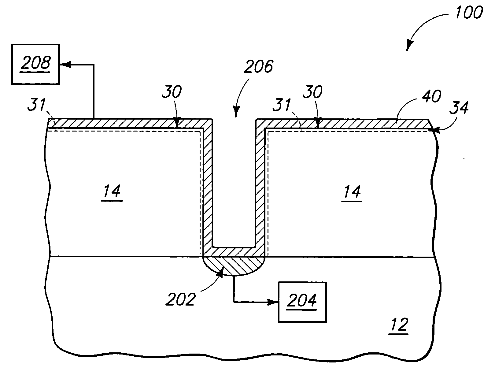
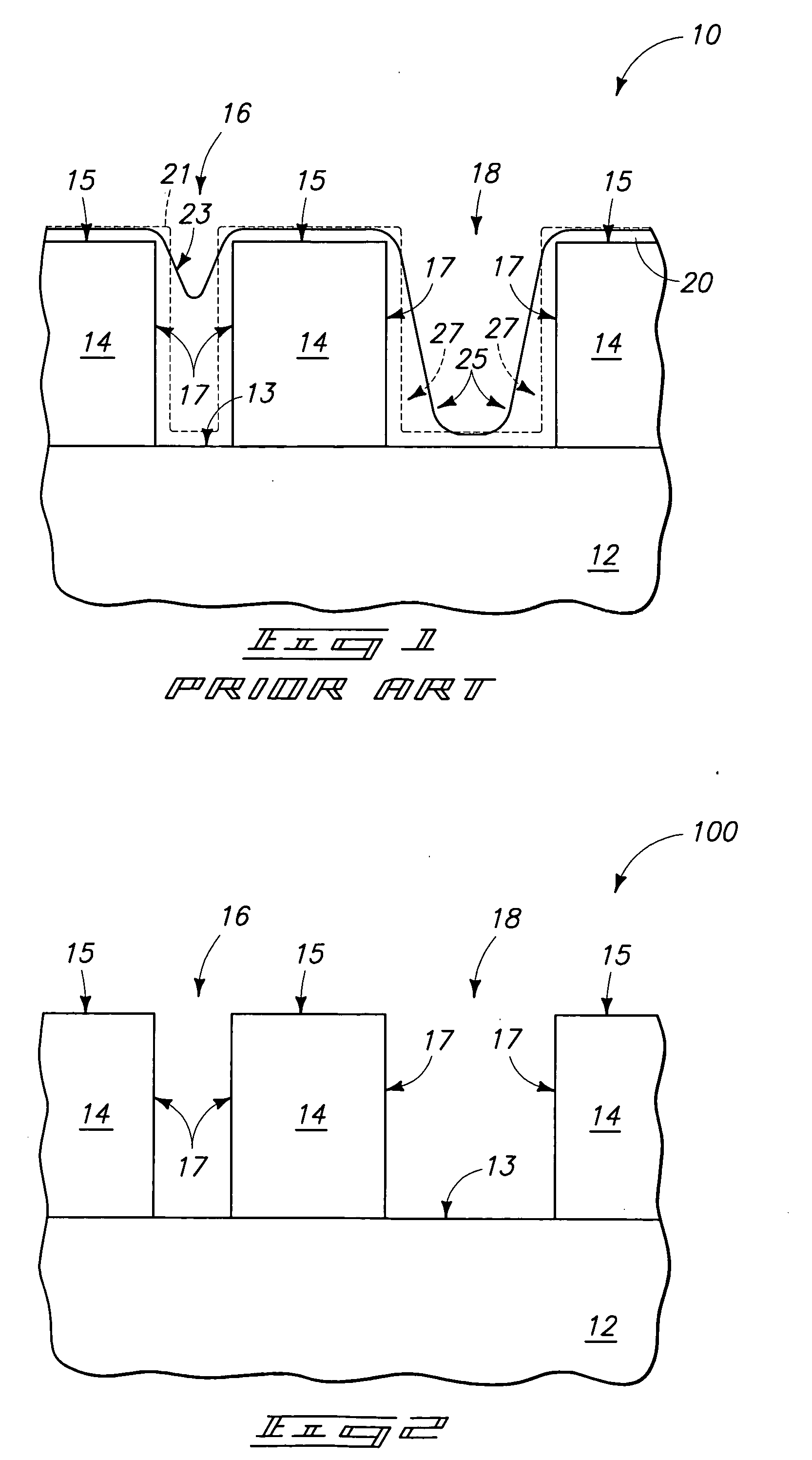
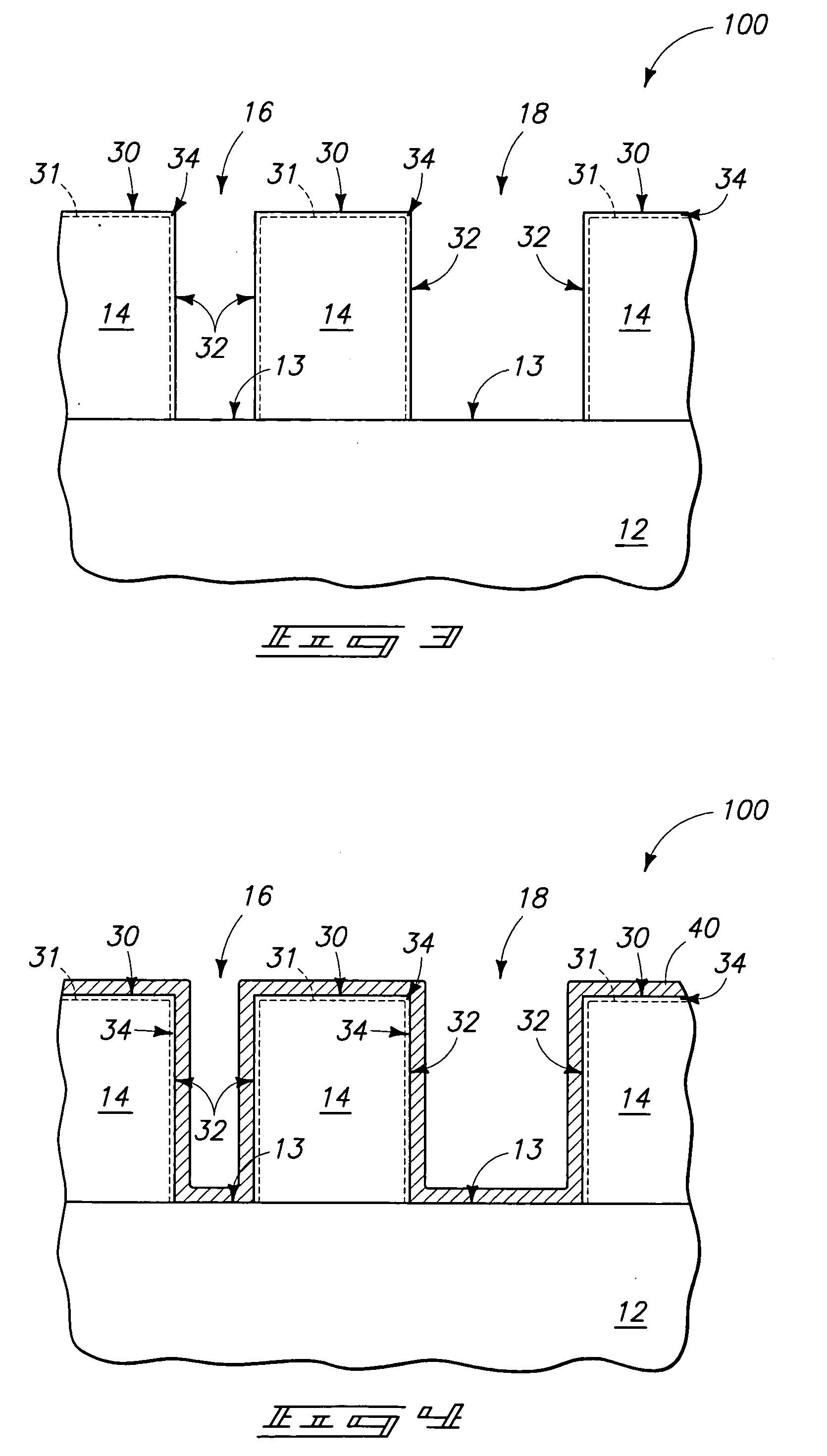
[0025] The invention includes utilization of surface modification to enable formation of conformal electrically conductive layers across semiconductor substrates. In particular aspects, a semiconductor construction having a patterned electrically insulative material is immersed in a liquid comprising one or more of titanium oxide, yttrium oxide, zirconium oxide, vanadium oxide and neodymium oxide to create a surface modification layer. The construction is then spin-coated with a metal silane or metal silazane precursor to form a metal-containing layer across the construction, and conformally across a surface of the patterned insulative material. In particular aspects, methodology of the present invention can be for utilized for pitch-doubling definition of conductive layers, and / or for ...


PUM

PropertyMeasurementUnit
temperatureaaaaaaaaaa

Abstract

The invention includes methods of forming layers conformally over undulating surface topographies associated with semiconductor substrates. The undulating surface topographies can first be exposed to one or more of titanium oxide, neodymium oxide, yttrium oxide, zirconium oxide and vanadium oxide to treat the surfaces, and can be subsequently exposed to a material that forms a layer conformally along the treated surfaces. The material can, for example, comprise one or both of aluminum silane and aluminum silazane. The invention also includes semiconductor constructions having conformal layers formed over liners containing one or more of titanium oxide, yttrium oxide, zirconium oxide and vanadium oxide.

Description

TECHNICAL FIELD [0001] The invention pertains to semiconductor constructions, and to methods of forming layers, such as, for example, layers associated with semiconductor constructions. BACKGROUND OF THE INVENTION [0002] Semiconductor processing can involve fabrication of various circuit devices over a semiconductor substrate, (such as, for example, a semiconductor wafer substrate) to form integrated circuitry. Semiconductor processing frequently involves formation of thin layers or films, with such layers or films ultimately being incorporated into various integrated circuit features. [0003] Problems can occur during the formation of layers. For instance, it can be desired for layers to be relatively conformal across an undulating topography, and yet it is found that it is very difficult in practice to form a conformal layer across a complex topography using coating type methods. Such problem is illustrated in FIG. 1 which shows a semiconductor construction 10 formed in accordance ...

Claims


Application Information

Patent Timeline
Patent Type & Authority Applications(United States)
IPC IPC(8): H01L21/4763
CPCH01L21/288H01L21/316H01L21/76877H01L21/76831H01L21/76843H01L21/32051H01L21/02222H01L21/02126H01L21/02211
Inventor SMYTHE, JOHN
Owner MICRON TECH INC
Why Eureka
Try Eureka