

Organic Light-Emitting Diodes and an Arrangement with Several Organic Light-Emitting Diodes
- Summary
- Abstract
- Description
- Claims
- Application Information
AI Technical Summary
Benefits of technology
Problems solved by technology
Method used
Image

Examples
embodiment example 1
[0062] An embodiment for a blue-emitting OLED comprises the following layers: [0063]1 Substrate, aluminium foil [0064]2 Silver layer, sputtered [0065]3 Hole transport layer. Spiro-TTB, p-doped with 2% NDP-2, 35 nm thick [0066]4 Electron block layer, Spiro-TAD, 10 nm [0067]5 Emitter layer—blue emitter, 20 nm [0068]6 Electron transport layer, BPhen, 10 nm [0069]7 Electron transport layer, BPhen, n-doped with Cs in the ratio 1:1, 130 nm [0070]8 Transparent cathode, Ag vapour-deposited, 15 nm
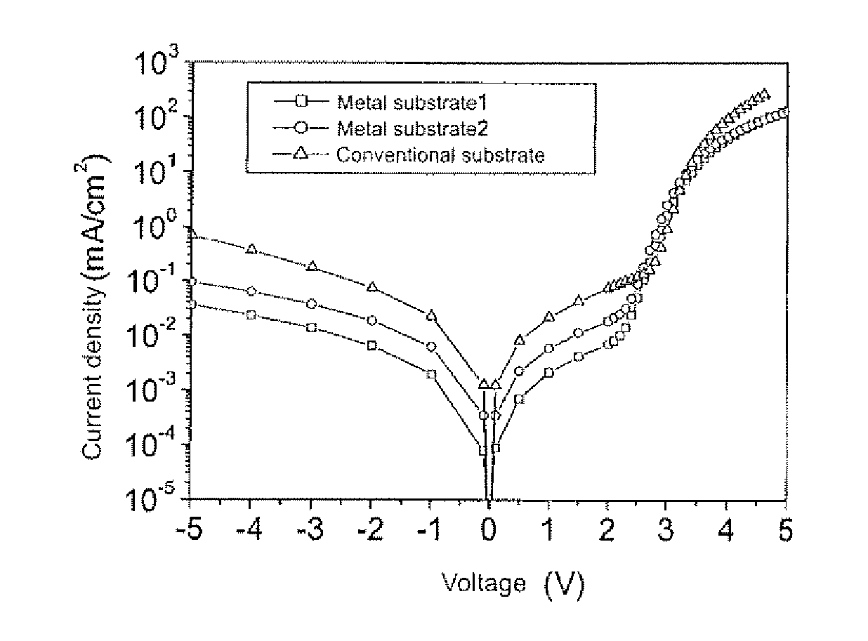
[0071]FIG. 1 shows a current-voltage characteristic curve of two organic light-emitting components of this type (squares and circles); as a comparison to this, a similar component (triangles) is shown that was realised on a high-quality glass substrate with a Cr / Ag-contact produced under clean room conditions. It is obvious that the OLEDs have blocking characteristic curves that are significantly better. The surprising aspect here is the fact that this effect merely requires an unusually thick elec...
embodiment example 2
[0072] An embodiment for a green-emitting OLED comprises the following layers: [0073]10 Substrate, aluminium foil [0074]11 Silver layer, sputtered [0075]12 Hole transport layer: Spiro-TTB, p-doped with 2% NDP-2, 48 nm thick [0076]13 Electron block layer, Spiro-TAD, 10 nm [0077]14 Emitter layer I, TCTA: Ir(ppy)3 (9%), 5 nm [0078]15 Emitter layer IT, TPBI: Ir(ppy)3 (9%), 10 nm [0079]16 Electron transport layer, BPhen, 10 nm [0080]17 Electron transport layer, BPhen, n-doped with Cs in the ratio 1:1, 130 nm [0081]18 Transparent cathode, Ag vapour-deposited, 15 nm [0082]19 Cover layer: Spiro-TTB, 90 nm
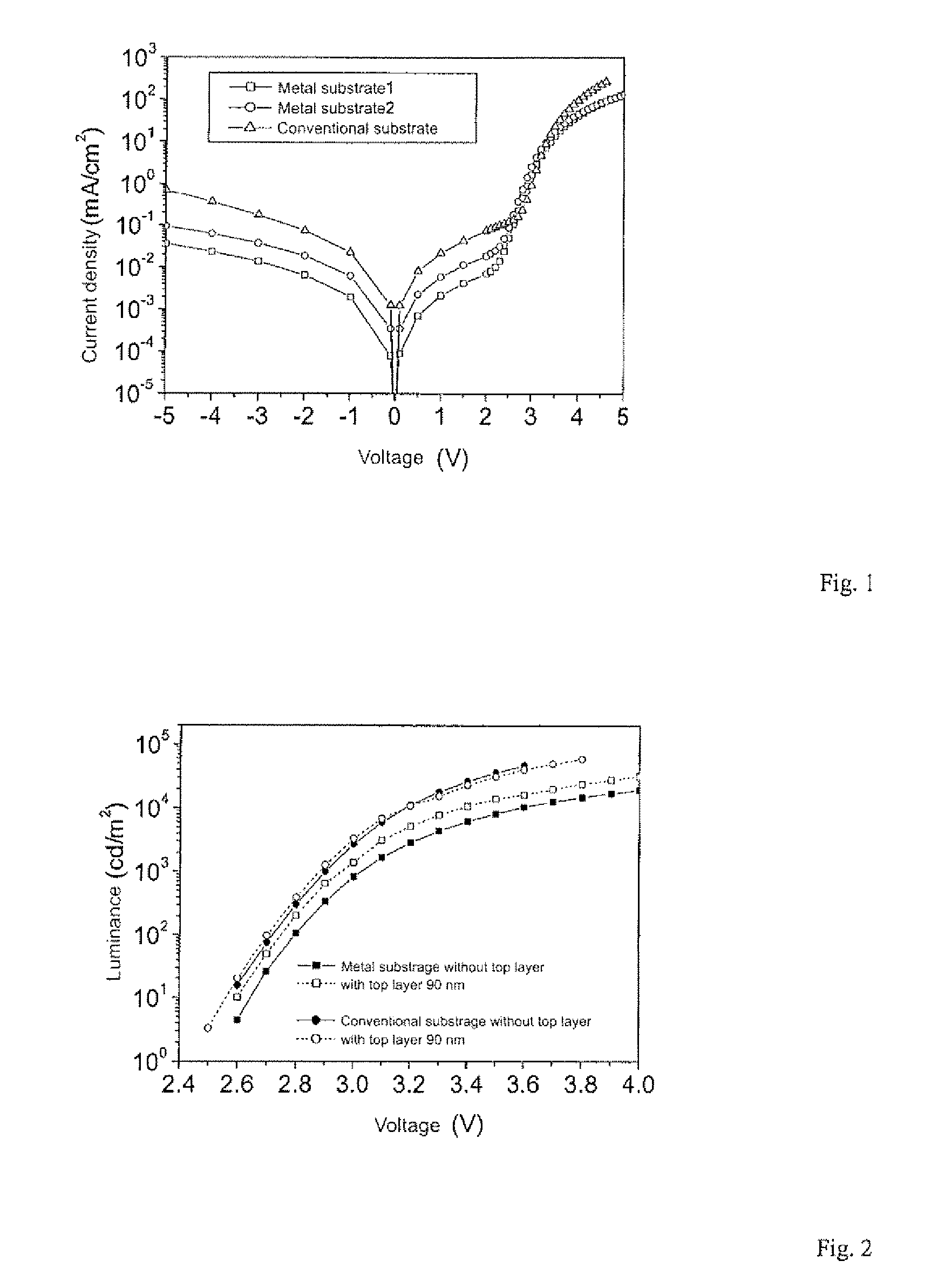
[0083]FIG. 2 shows a luminance-voltage characteristic curve of two organic light-emitting components according to the second embodiment (squares and circles, each with and without layer 19). The brightness of 100 Cd / m2 is already obtained at 2.9 V, the maximum performance efficiency is 50 lm / W at 10,000 Cd / m2. This shows that OLEDs can be realised with excellent parameters on metallic subs...
embodiment example 3
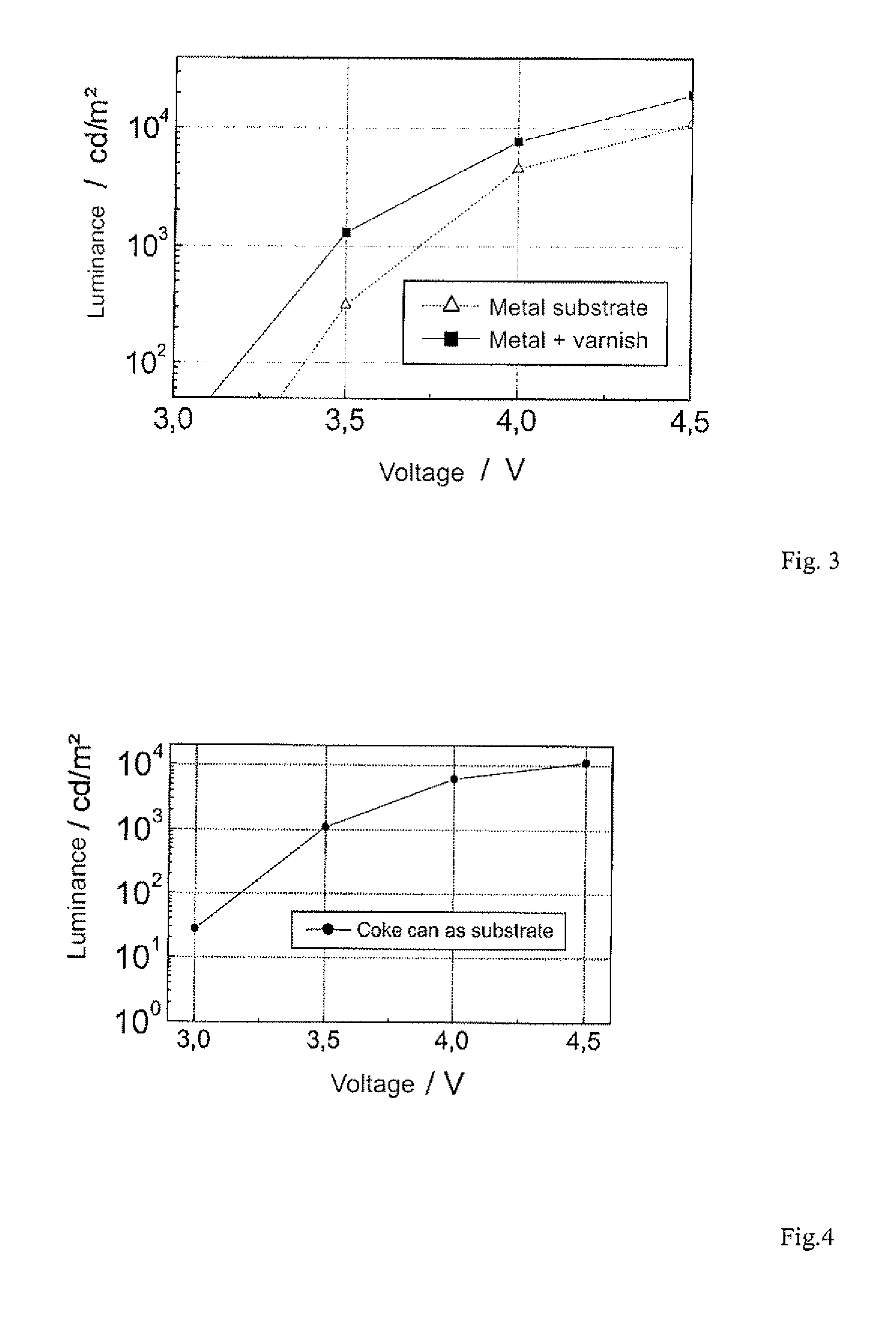
[0085] In an embodiment 3, it is shown how an additional varnish layer on a metal substrate contributes to reduced leakage currents and, subsequently, to improved electrical properties. At the same time, a thick p-side is used which contributes towards a further homogenisation of the surface. For this purpose, FIG. 3 compares two OLEDs that are similar in design with the following structure where one was executed with and one was executed without a smoothening layer 21. [0086]20 Substrate, aluminium foil, [0087]21 Smoothening layer, varnish (optional) [0088]22 Silver layer, sputtered [0089]23 Hole transport layer: MeO-TPD, p-doped with 4% F4-TCNQ, 150 nm thick [0090]24 Electron block layer, Spiro-TAD, 10 nm [0091]25 Emitter layer, TCTA: Ir(ppy)3 (8%), 20 nm [0092]26 Electron transport layer, BPhen, 10 nm [0093]27 Electron transport layer, BPhen, n-doped with Cs in the ratio 1:1, 30 nm [0094]28 Transparent cathode, Ag vapour-deposited, 15 nm
[0095] As can be seen in FIG. 3, a further...
PUM
 Abstract
Description
Claims
Application Information