Semiconductor laser device
- Summary
- Abstract
- Description
- Claims
- Application Information
AI Technical Summary
Benefits of technology
Problems solved by technology
Method used
Image

Examples
first embodiment
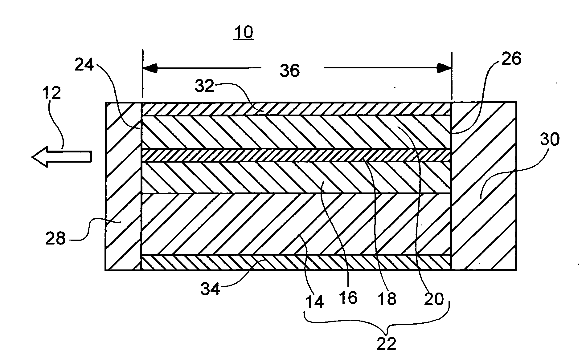
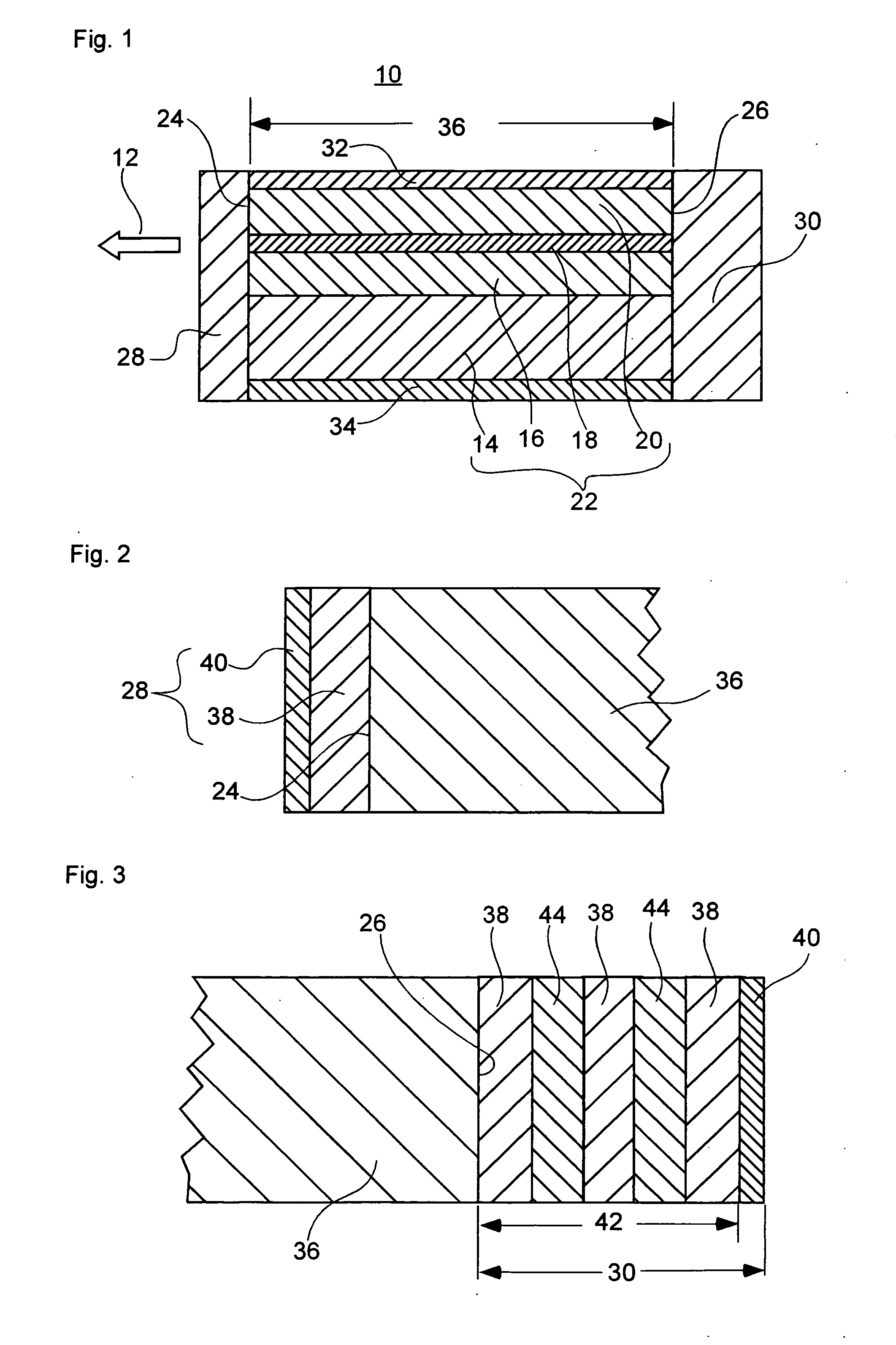
[0035]FIG. 1 is a cross-sectional view of a semiconductor laser according to one embodiment of the present invention. It should be noted that like numerals indicate like or corresponding components throughout FIG. 1 and the following figures.
[0036] Specifically, FIG. 1 shows a cross section of a semiconductor laser 10 taken along a plane parallel to the waveguide direction of the semiconductor laser. In the figure, the arrow indicates exiting light 12 from the semiconductor laser 10.
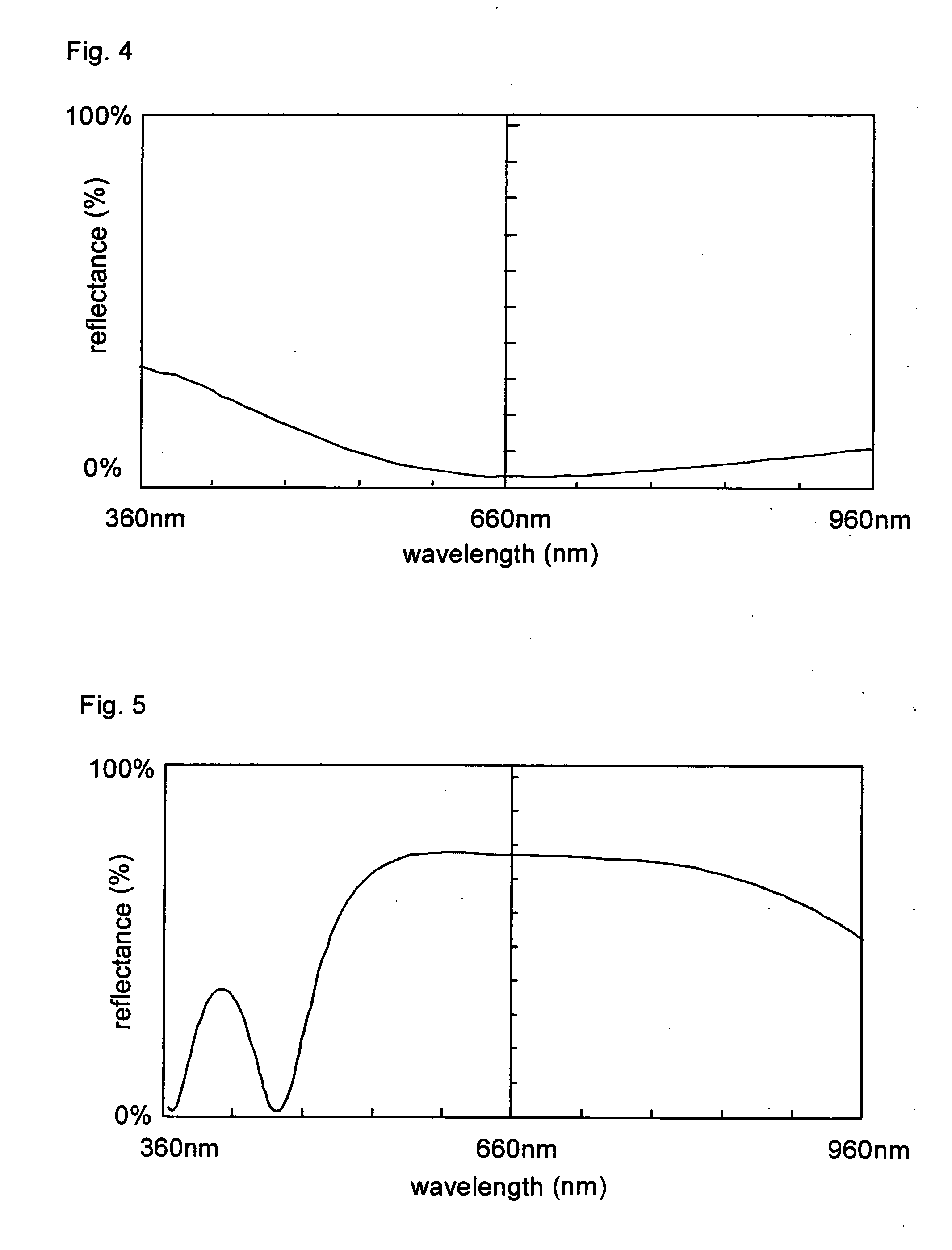
[0037] The semiconductor laser 10 may be, for example, a red semiconductor laser having an oscillation wavelength of 660 nm.
[0038] The semiconductor laser 10 includes an n-type GaAs substrate 14, an n-type cladding layer 16, an active layer 18, and a p-type cladding layer 20. The n-type cladding layer 16, the active layer 18, and the p-type cladding layer 20, which together constitute a resonator 22, are sequentially formed over the n-type GaAs substrate 14. Further, a p-electrode 32 is disposed on th...
PUM
 Abstract
Description
Claims
Application Information
 - Generate Ideas
- Intellectual Property
- Life Sciences
- Materials
- Tech Scout
- Unparalleled Data Quality
- Higher Quality Content
- 60% Fewer Hallucinations
Browse by: Latest US Patents, China's latest patents, Technical Efficacy Thesaurus, Application Domain, Technology Topic, Popular Technical Reports.
© 2025 PatSnap. All rights reserved.Legal|Privacy policy|Modern Slavery Act Transparency Statement|Sitemap|About US| Contact US: help@patsnap.com