Method and apparatus for reviewing defects

Inactive Publication Date: 2007-03-15
HITACHI HIGH-TECH CORP
View PDF10 Cites 87 Cited by
  • Summary
  • Abstract
  • Description
  • Claims
  • Application Information

AI Technical Summary

Benefits of technology

[0012] When the defect detected by the optical foreign matter inspection apparatus or the optical appearance inspection apparatus is reviewed in detail by using the SEM, the invention makes it possible to reliably bring the defect de

Problems solved by technology

Foreign matters, if any, on a semiconductor substrate (wafer) may result in defects such as inferior insulation and short-circuit of wiring in a semiconductor production process.
With miniaturization of semiconductor chips, finer foreign matters may result in insulation defects of capacitors and breakdown of a gate oxide film.
Therefore, accuracy of the position coordinates determined from the position of the laser beam spot that scans the semiconductor substrate surface contains a large error component.
To bring the image of the defect to be reviewed into the visual field of the SEM in such a case, the defect is searched out while being moved inside the visual field of the SEM, but this is time consuming and results in the drop of through-put of the SEM observati

Method used


Image

  • Method and apparatus for reviewing defects
  • Method and apparatus for reviewing defects
  • Method and apparatus for reviewing defects

Examples


Embodiment Construction

[0036] Preferred embodiments of the invention will be hereinafter explained with reference to the accompanying drawings.

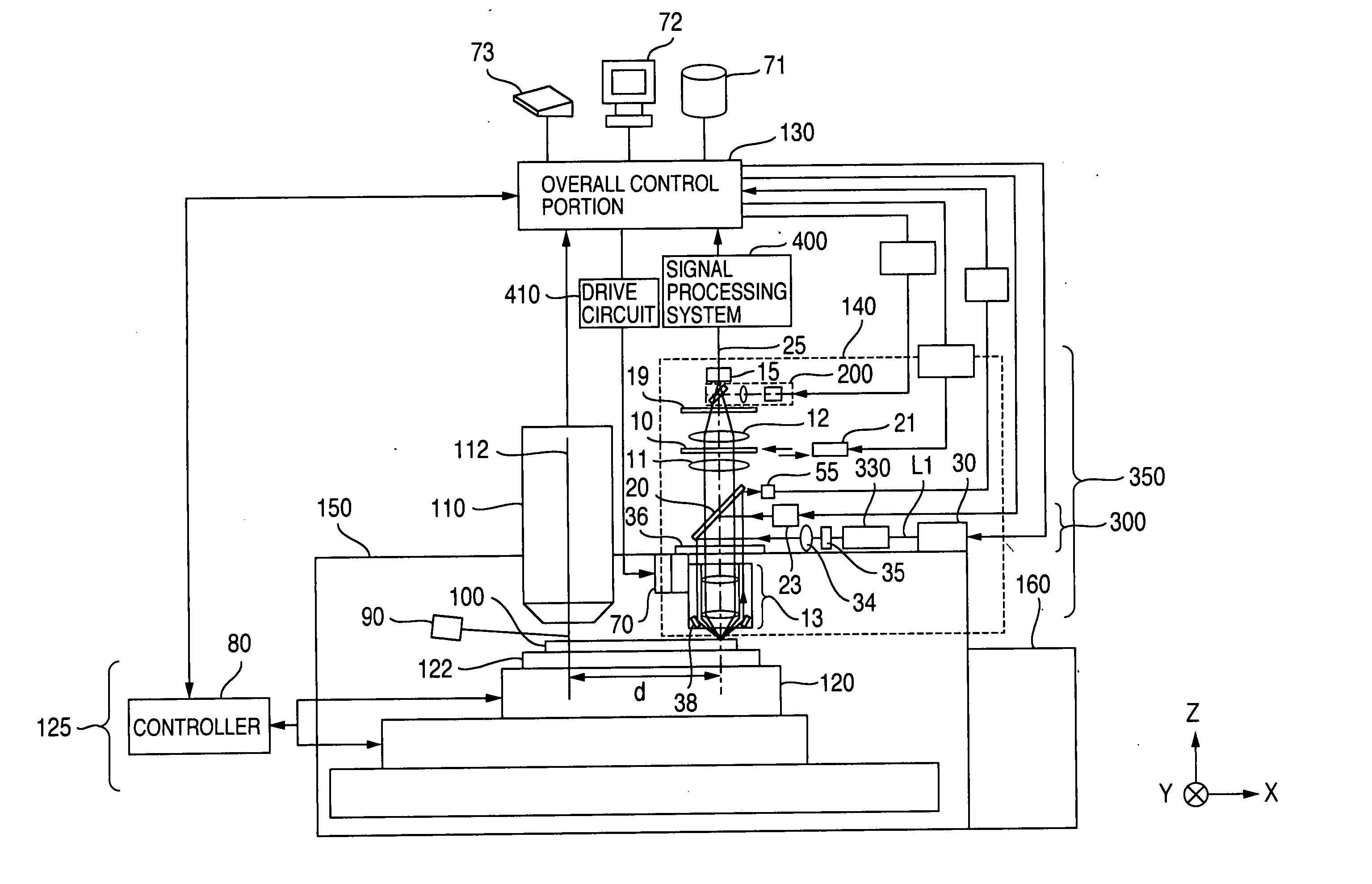
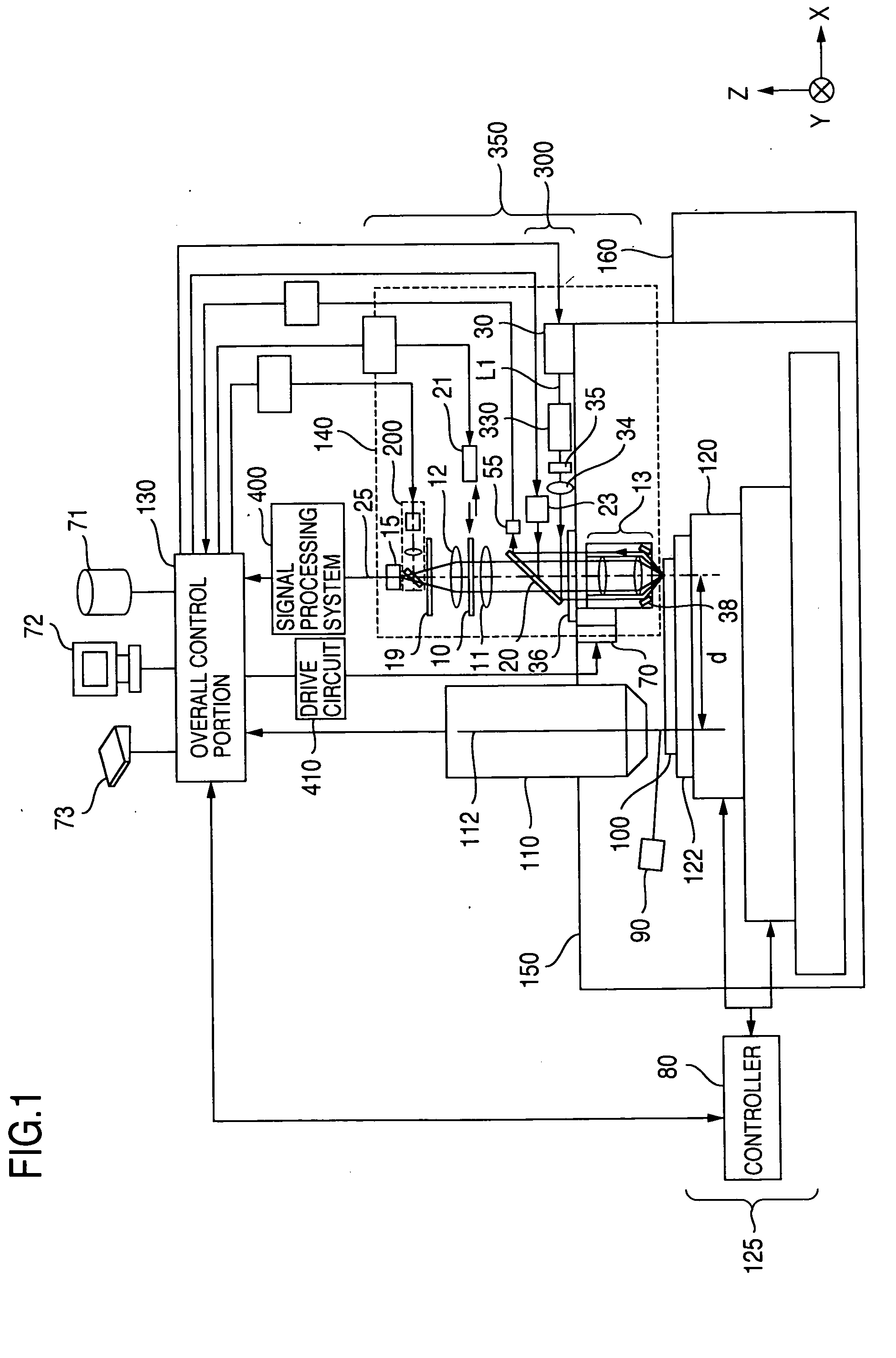
[0037] A defect reviewing apparatus on an article surface according to the invention includes a scanning electron microscope (SEM) 110, a defect detection device 140, a conveyor system 125, a load lock chamber 160 having these members assembled therein, a vacuum chamber 150 having vacuum exhaust means not shown, and an overall control portion 130 as shown in FIG. 1.

[0038] The conveyor system 125 includes an XY stage 120 for placing and moving reviewing object substrates 100 fabricated from various production processes such as wafers, and a controller 80.

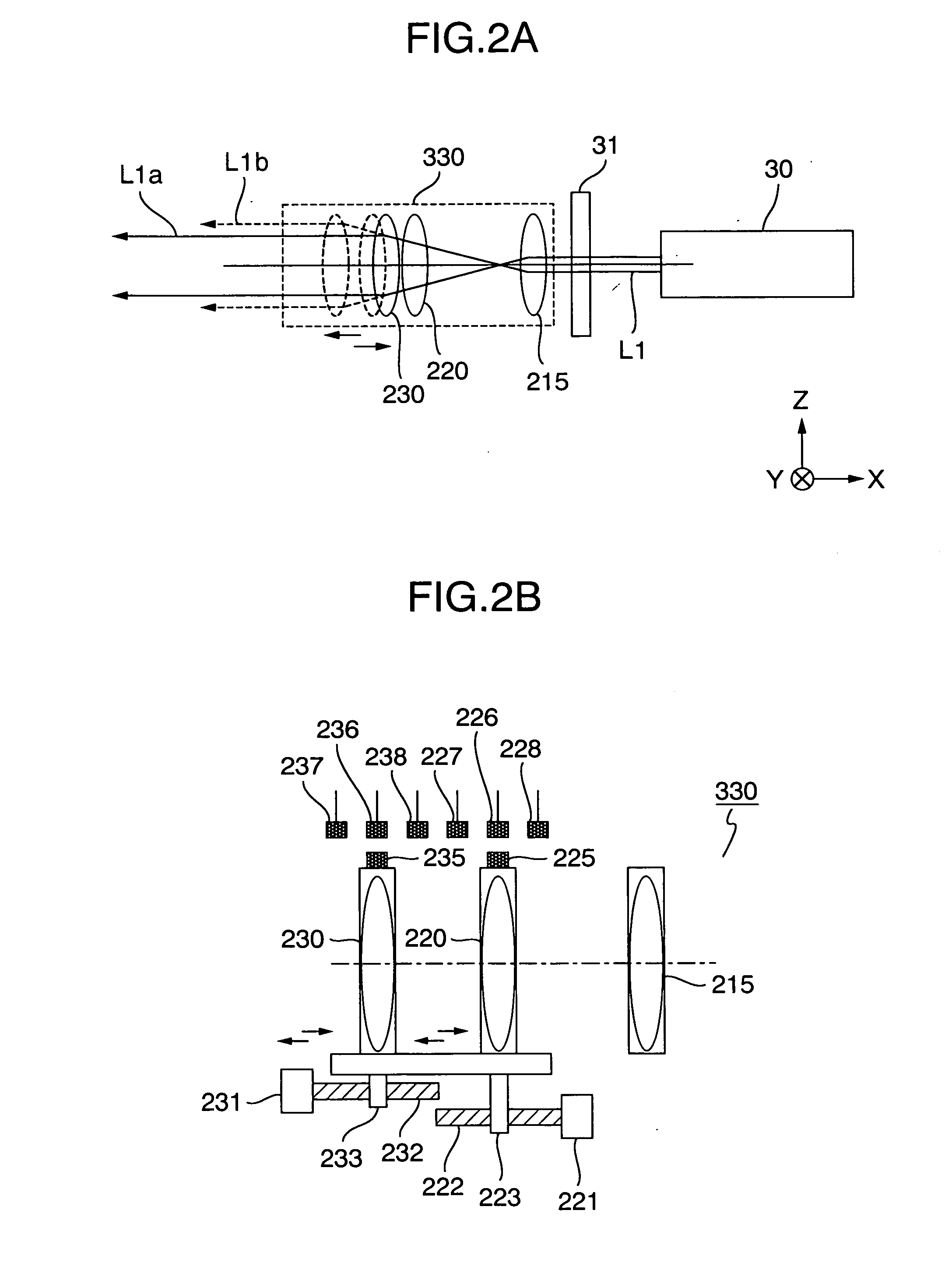
[0039] The defect reviewing apparatus 140 includes a dark visual field illumination system 300 for setting a laser beam L1 outgoing from a laser beam source 30 to a certain size by beam diameter varying means 330 and then irradiating the laser beam from an obliquely upward direction of the reviewing object substr...


PUM


Abstract

The invention provides an apparatus and a method each capable of highly accurately reviewing at a high speed very small foreign matters and pattern defects occurring during a device production process for forming a circuit pattern on a substrate of semiconductor devices, etc. An objective lens having high NA is installed inside a vacuum chamber for an inspection object having a transparent film formed on the surface thereof and an illumination optical path is formed inside the objective lens so that dark visual field illumination can be made and reflected and scattered light of foreign matters or defects on the surface of the inspection object can be detected with high sensitivity.

Description

INCORPORATION BY REFERENCE [0001] The present application claims priority from Japanese application JP2005-261563 filed on Sep. 9, 2005, the content of which is hereby incorporated by reference into this application. BACKGROUND OF THE INVENTION [0002] This invention relates to a method for reviewing a defect occurring in a semiconductor production process and an apparatus for the method. More particularly, the invention relates to a method for reviewing a defect, and an apparatus for the method, that will be suitable for reviewing in detail a defect by using an electron microscope. [0003] Foreign matters, if any, on a semiconductor substrate (wafer) may result in defects such as inferior insulation and short-circuit of wiring in a semiconductor production process. With miniaturization of semiconductor chips, finer foreign matters may result in insulation defects of capacitors and breakdown of a gate oxide film. These foreign matters are generated for various causes such as those whi...

Claims


Application Information

Patent Timeline
IPC IPC(8): H01J37/22G01N21/01H01J37/28
CPCG01N21/95607G01N21/95623G01N2021/8825G06T7/001H01J2237/2817G06T2207/30148H01J37/226H01J37/28G06T2207/10061
Inventor UTO, SACHIOMAEDA, SHUNJI
Owner HITACHI HIGH-TECH CORP
Why Eureka
Try Eureka