Method for manufacturing semiconductor memory device using asymmetric junction ion implantation

a semiconductor memory and asymmetric junction technology, applied in the direction of semiconductor devices, basic electric elements, electrical appliances, etc., can solve the problems of deteriorating device operating characteristics and stability, and deteriorating device refresh characteristics, so as to prolong data retention time and improve refresh characteristics

Inactive Publication Date: 2007-03-22
SK HYNIX INC
View PDF3 Cites 8 Cited by
  • Summary
  • Abstract
  • Description
  • Claims
  • Application Information

AI Technical Summary

Benefits of technology

[0008] The invention provides a method for manufacturing a semiconductor memory device, which can actively induce asymmetric distribution in concentration between a storage node junction region and a bit line junction region, thereby improving refresh characteristics while extending data retention time.

Problems solved by technology

As the channel length is decreased, operating characteristics of the device deteriorate due to various problems caused by a short channel effect.
For example, a decrease of the channel length causes an increase in intensity of electric field near a drain region, which in turn generates hot carriers, thereby deteriorating the operating characteristics and stability of the device.
In another example, for a semiconductor memory device such as dynamic random access memory (DRAM), the increase in intensity of electric field in a cell region causes current leakage, which in turn deteriorates refresh characteristics of the device.
However, it is difficult for the conventional method of asymmetric threshold voltage ion implantation to satisfy such requirements.

Method used


Image

  • Method for manufacturing semiconductor memory device using asymmetric junction ion implantation
  • Method for manufacturing semiconductor memory device using asymmetric junction ion implantation
  • Method for manufacturing semiconductor memory device using asymmetric junction ion implantation

Examples


first embodiment

[0054] FIGS. 1 to 4 are cross-sectional views illustrating a method for manufacturing a semiconductor memory device in accordance with the invention. In this embodiment, the method can be applied to a semiconductor memory device having a planar structure.

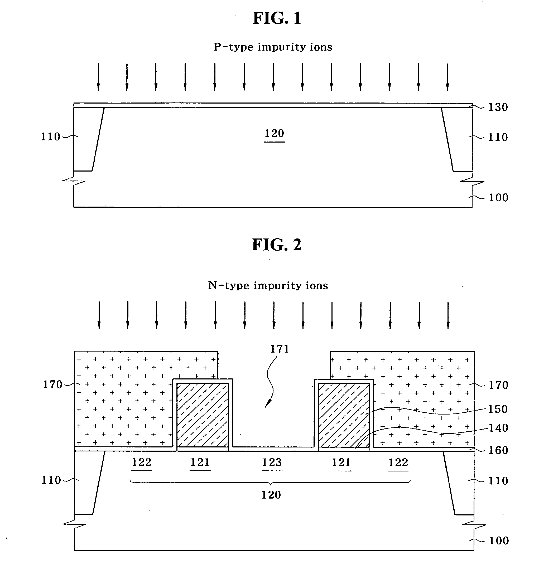
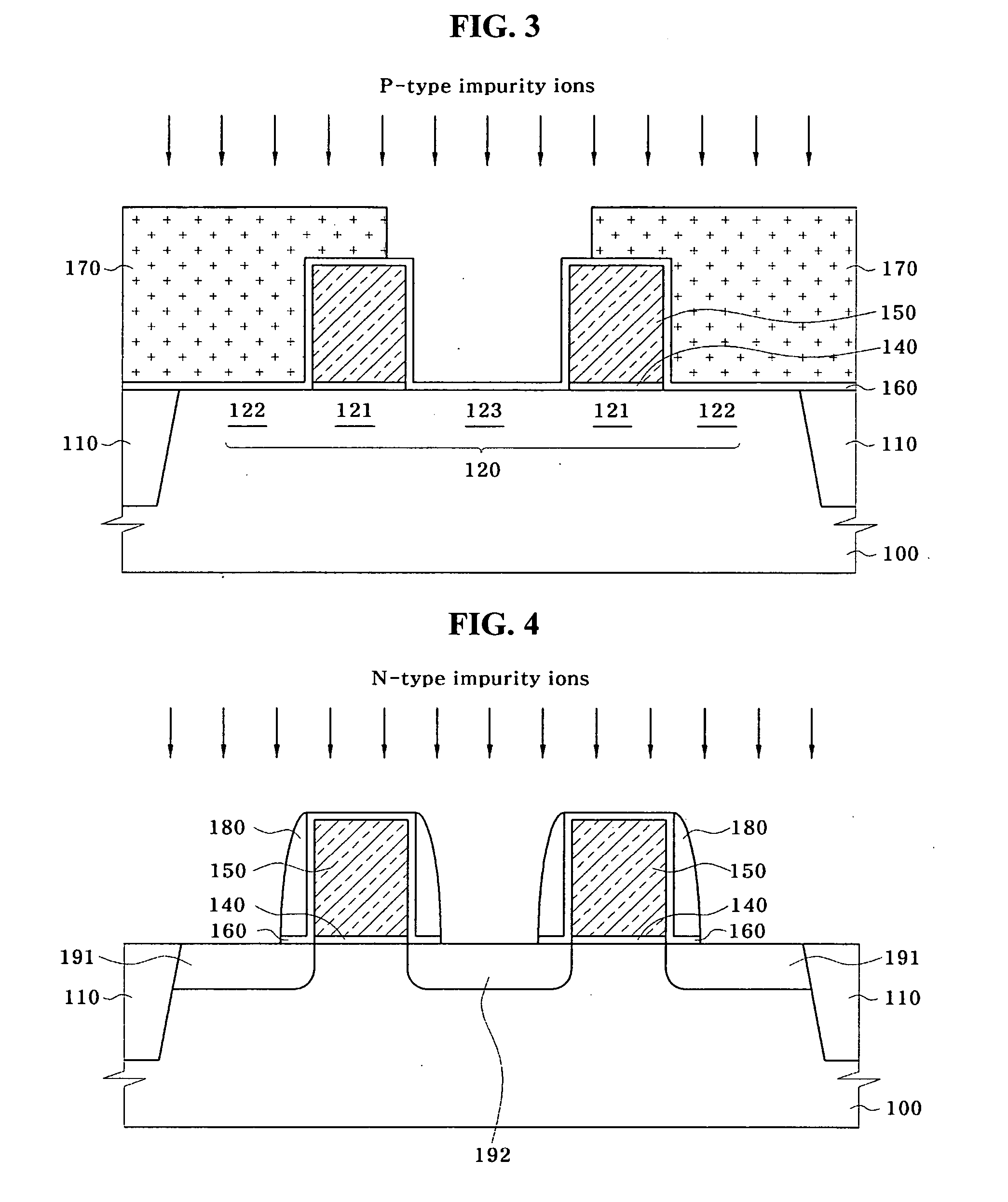
[0055] Referring to FIG. 1, an active region 120 is defined by forming isolation layers 110 on a semiconductor substrate 100. Then, a buffer insulation layer 130 is formed of an oxide layer on the semiconductor substrate 100 having the active region 120 defined thereon. Next, as indicated by arrows in FIG. 1, ion implantation for channel threshold voltage is performed on an overall surface of the semiconductor substrate 100. This embodiment will be described using an n-type channel as an example. Accordingly, p-type impurity ions are implanted to an upper portion of the semiconductor substrate 100 by the ion implantation for channel threshold voltage. The p-type impurity ions are implanted in a concentration about 70% of an entire c...

second embodiment

[0062] Now referring to FIG. 5, an active region is defined by forming isolation layers 210 on a semiconductor substrate 200. Then, trenches 201 and 202 for a recess channel are formed by etching a portion of the active region on the semiconductor substrate 200 by a predetermined depth. As the trenches 201 and 202 for the recess channel are formed, the active region of the semiconductor substrate is defined with a channel region formed along the trenches 201 and 202 for the recess channel, a storage node junction region 122, and a bit line junction region 123. Then, a buffer insulation layer 230 is formed of an oxide layer on the semiconductor substrate 200 having the trenches 201 and 202 for the recess channel formed thereon. In some cases, a natural oxide layer may be used as the buffer insulation layer 230. Next, as indicated by arrows in FIG. 5, ion implantation for channel threshold voltage is performed on the overall surface of the semiconductor substrate 200. The second embod...

third embodiment

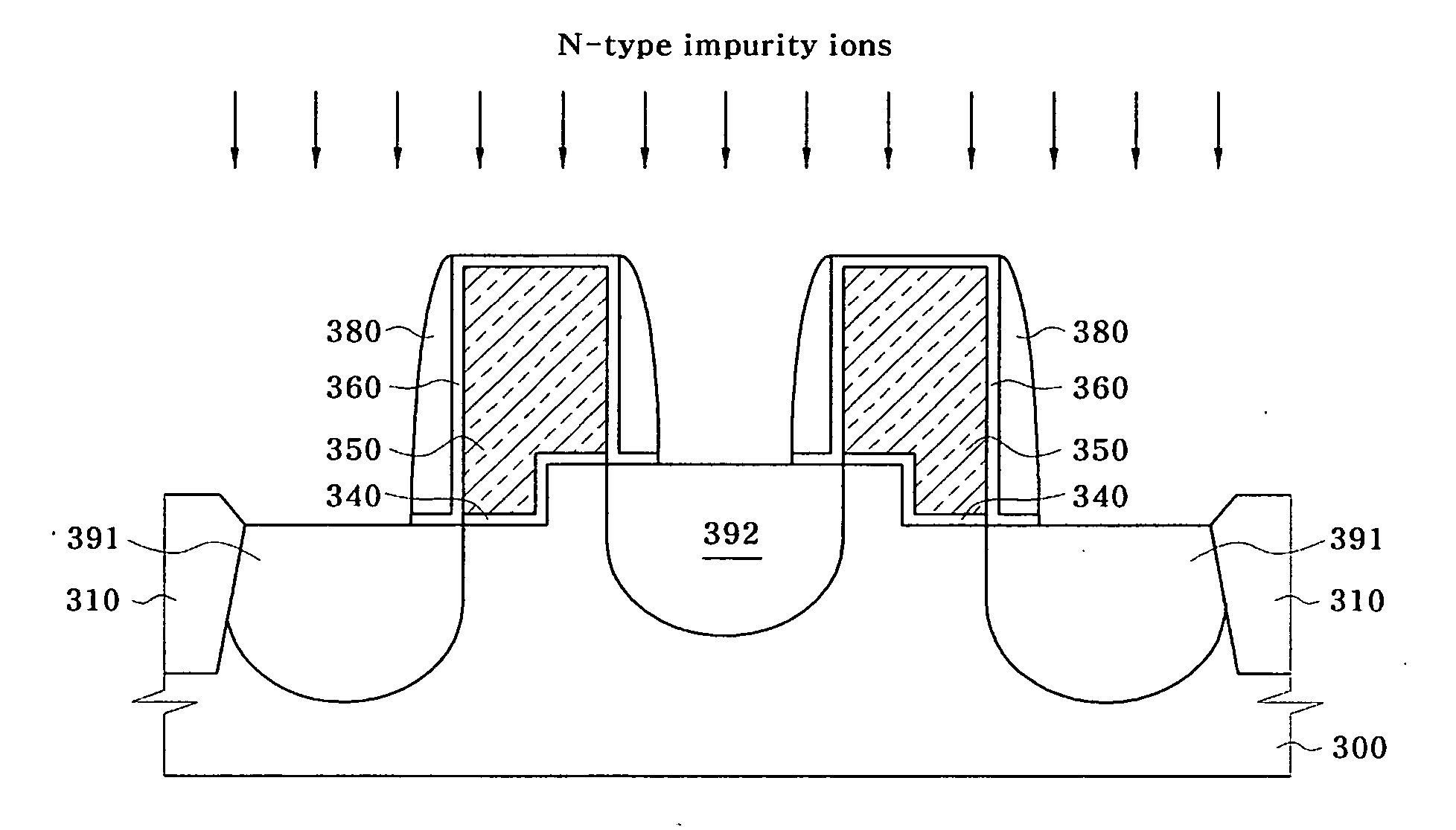
[0069] Now referring to FIG. 9, an active region is defined by forming isolation layers 310 on a semiconductor substrate 300. Then, a step profile is formed by etching a portion of the active region on the semiconductor substrate 300 by a predetermined depth. Then, as indicated by arrows in FIG. 9, ion implantation for channel threshold voltage is performed on an overall surface of the semiconductor substrate 300 having the step profile formed thereon. Although not shown in the drawing, a natural oxide layer or an additional buffer insulation layer may be disposed on the semiconductor substrate 300. The third embodiment will also be described using an n-type channel as an example. Accordingly, p-type impurity ions are implanted to an upper portion of the semiconductor substrate 300 by the ion implantation for channel threshold voltage. The p-type impurity ions are implanted in a concentration about 70% of an entire channel concentration.

[0070] Referring to FIG. 10, a gate insulation...


PUM


Abstract

A method for manufacturing a semiconductor memory device using asymmetric junction ion implantation, including performing ion implantation for adjusting a threshold voltage to a semiconductor substrate, forming a gate stack on the semiconductor substrate to define a storage node junction region and a bit line junction region, implanting a first conductive impurity ion and a second conductive impurity ion using a mask layer pattern covering the storage node junction region while exposing the bit line junction region, forming a gate spacer layer at both sides of the gate stack, and implanting the first conductive impurity ion using the gate stack and the gate spacer layer as an ion implantation mask layer to form a storage node junction region and a bit line junction region having different impurity concentrations, and different junction depths from each other.

Description

BACKGROUND OF THE INVENTION [0001] 1. Field of the Invention [0002] The invention relates generally to a method for manufacturing a semiconductor memory device and, more particularly, to a method for manufacturing a semiconductor memory device using asymmetric junction ion implantation. [0003] 2. Description of the Related Art [0004] Rapid development in the technology of increasing the degree of integration on semiconductor memory devices has caused a rapid decrease in channel length of transistors in such devices. As the channel length is decreased, operating characteristics of the device deteriorate due to various problems caused by a short channel effect. For example, a decrease of the channel length causes an increase in intensity of electric field near a drain region, which in turn generates hot carriers, thereby deteriorating the operating characteristics and stability of the device. In another example, for a semiconductor memory device such as dynamic random access memory (D...

Claims


Application Information

Patent Timeline
Patent Type & Authority Applications(United States)
IPC IPC(8): H01L21/338H01L21/8234H01L21/336
CPCH01L27/10855H01L27/10876H01L29/66659H01L29/1037H01L29/66621H01L27/10888H10B12/053H10B12/485H10B12/0335H10B99/00
Inventor LEE, MIN YONGROUH, KYOUNG BONGJIN, SEUNG WOO
Owner SK HYNIX INC
Why Eureka
Try Eureka