Method for manufacturing semiconductor device

Inactive Publication Date: 2007-03-29
PS4 LUXCO SARL
View PDF2 Cites 19 Cited by
  • Summary
  • Abstract
  • Description
  • Claims
  • Application Information

AI Technical Summary

Benefits of technology

[0006] An object of the present invention is therefore to overcome the drawback of photo-resist residue, and to provide a method for manufacturing a semiconductor device whereby

Problems solved by technology

However, short channel effects in a transistor become more severe as the gate length is shortened, and drawbacks occur whereby the threshold voltage (Vt) of the transistor is reduced by increased sub-threshold current.
When the impurity concentration in the substrate is increased in order to minimize the decrease in Vt, deterioration of the refresh characterist

Method used


Image

  • Method for manufacturing semiconductor device
  • Method for manufacturing semiconductor device
  • Method for manufacturing semiconductor device

Examples


first embodiment

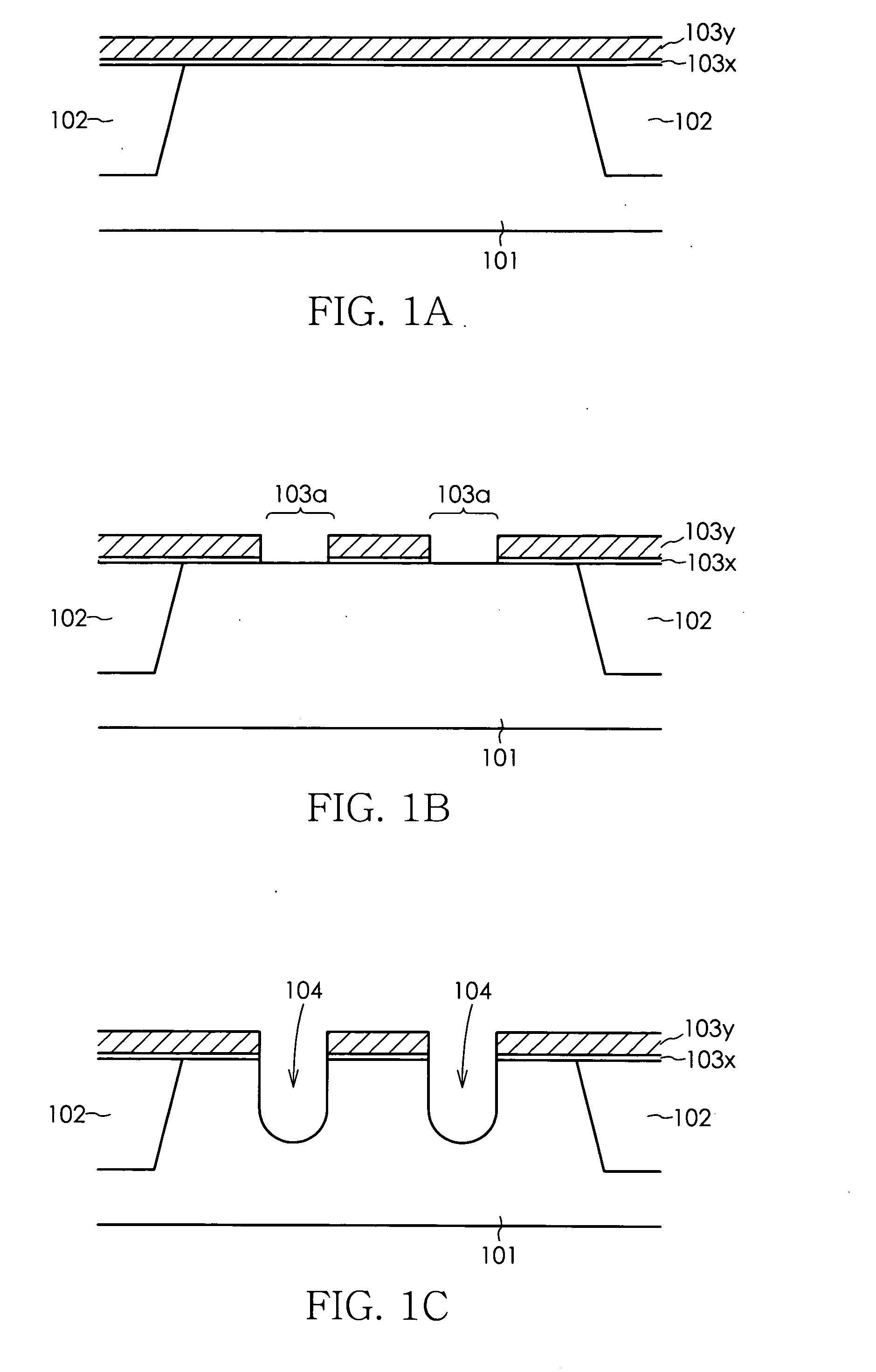
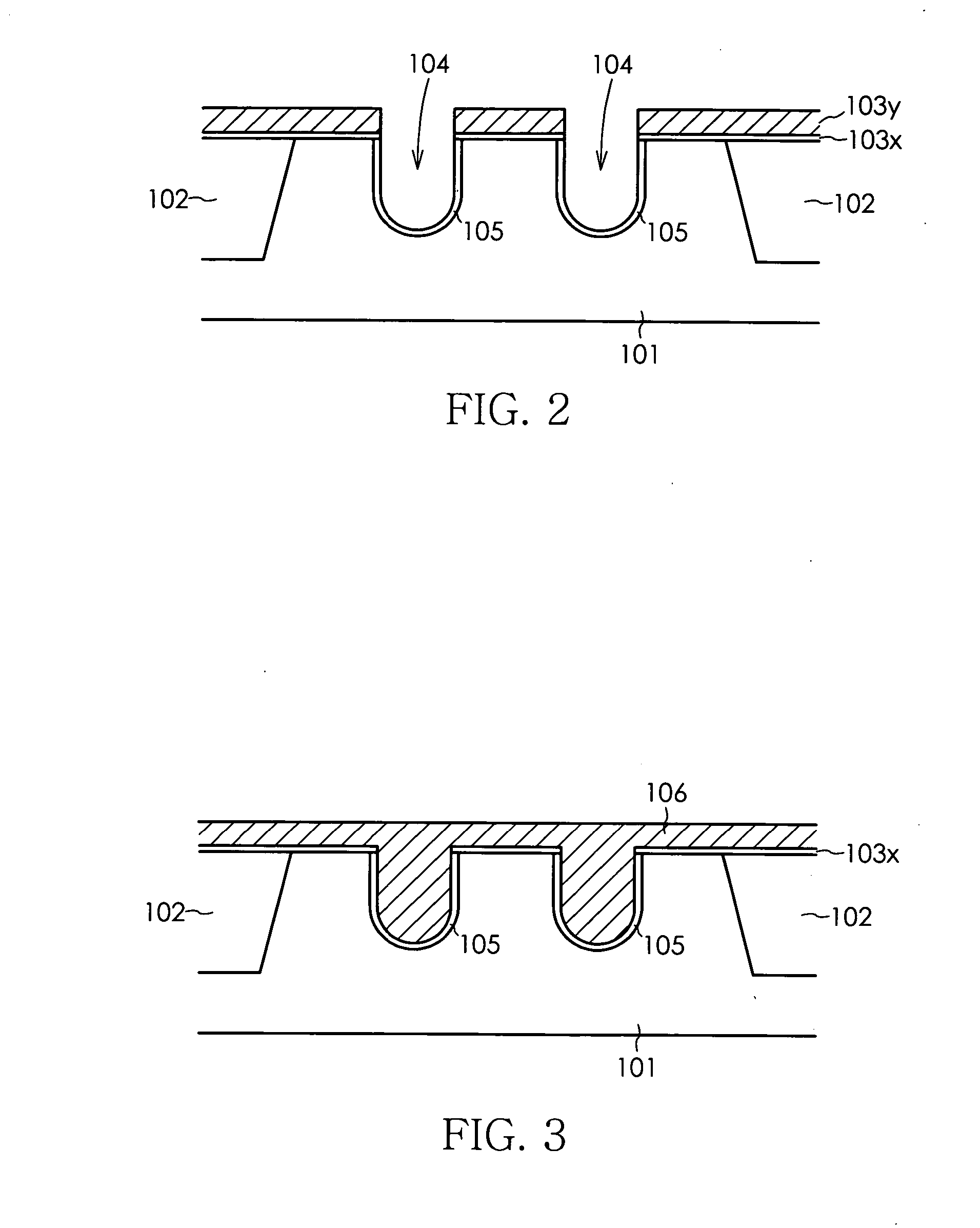
[0033]FIGS. 1 through 8 are schematic cross sectional views or plan views showing the process for manufacturing DRAM according to the present invention.

[0034] In the DRAM manufacturing process according to the present embodiment, an element separation region 102 having a depth of about 250 to 350 nm is first formed by an STI (Shallow Trench Isolation) method on a P-type silicon substrate 101, after which a silicon oxide film 103x having a thickness of about 10 to 20 nm and a silicon nitride film 103y having a thickness of about 100 to 200 nm as protective insulating films are sequentially deposited by a CVD method on the surface of the silicon substrate 101 as shown in FIG. 1A. An opening 103a is then formed by using a photolithography to selectively remove the silicon nitride film 103y and silicon oxide film 103x in the prescribed region in which the gate electrode is to be formed, as shown in FIG. 1B, and a mask pattern is formed for use in forming a gate trench. Two grooves (gate...

second embodiment

[0044]FIGS. 9 through 11 are schematic cross sectional views and schematic plan views showing part of the process for manufacturing DRAM according to the present invention.

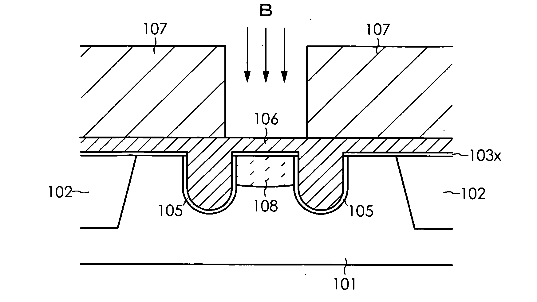
[0045] A feature of the present embodiment is that ion implantation for forming the bit-line-side source / drain region is first performed on a P-type silicon substrate 101 in which an element separation region 102 is formed, and then a sequence of steps is performed that includes gate electrode formation and other processes.

[0046] The step for forming a source / drain region on the bit line side is substantially the same as in the first embodiment. After a photo-resist 107 is first formed on the entire surface of a P-type silicon substrate 101, the photo-resist in the region in which the bit-line-side source / drain region is to be formed is selectively removed to form an opening 107a, and a mask pattern for ion implantation is formed, as shown in FIGS. 9A and 9B. FIG. 9A is a schematic plan view showing the process f...


PUM


Abstract

a method for manufacturing a semiconductor device comprises the steps of forming a gate trench in a semiconductor substrate, forming a gate insulation film in an inner wall of the gate trench, filling a gate electrode material into at least an inside of the gate trench, forming a gate electrode by patterning the gate electrode material, and selectively forming a punch-through stopper region prior to patterning the gate electrode material, using a mask in a prescribed position of the semiconductor substrate that is adjacent to the gate trench. The step for forming the punch-through stopper region may be performed subsequent to the step for filling the gate electrode material into the gate trench, or may be performed prior to the step for forming the gate trench.

Description

TECHNICAL FIELD [0001] The present invention relates to a method for manufacturing a semiconductor device, and particularly relates to a method for manufacturing a semiconductor device that is formed using a transistor having an asymmetrically structured source / drain region. BACKGROUND OF THE INVENTION [0002] The recent miniaturization of DRAM (Dynamic Random Access Memory) cells has been accompanied by the necessity of shortening the gate length of access transistors (hereinafter referred to as cell transistors) in cell arrays. However, short channel effects in a transistor become more severe as the gate length is shortened, and drawbacks occur whereby the threshold voltage (Vt) of the transistor is reduced by increased sub-threshold current. When the impurity concentration in the substrate is increased in order to minimize the decrease in Vt, deterioration of the refresh characteristics in the DRAM becomes a severe drawback because of increased junction leakage. [0003] Making the ...

Claims


Application Information

Patent Timeline
IPC IPC(8): H01L21/336
CPCH01L27/10876H01L29/1083H01L29/78H01L29/66659H01L29/66621H10B12/053
Inventor YAMAZAKI, YASUSHI
Owner PS4 LUXCO SARL
Why Eureka
Try Eureka