Method and program for designing semiconductor integrated circuits, and semiconductor integrated circuit designing apparatus

Inactive Publication Date: 2007-03-29
RENESAS ELECTRONICS CORP
View PDF1 Cites 7 Cited by
  • Summary
  • Abstract
  • Description
  • Claims
  • Application Information

AI Technical Summary

Benefits of technology

[0017] An object of the present invention is to provide a semiconductor integrated circuit designing method and designing apparatus which are capable of considering more realistic process variations during designing process so as to avoid setting of de

Problems solved by technology

Accordingly, if the value of on-chip variation is set too large in the design process in order to cover all possible circuit configurations, more margins than necessary will be ensured and performance and design convergence of semiconductor integrated circuits will be deteriorated.
On the other hand, if the on-chip variation value is set too small in design, necessary margin cannot be ensured and the possibility of malfunctions will increase.
As describ

Method used


Image

  • Method and program for designing semiconductor integrated circuits, and semiconductor integrated circuit designing apparatus
  • Method and program for designing semiconductor integrated circuits, and semiconductor integrated circuit designing apparatus
  • Method and program for designing semiconductor integrated circuits, and semiconductor integrated circuit designing apparatus

Examples


embodiment

Preferred Embodiment

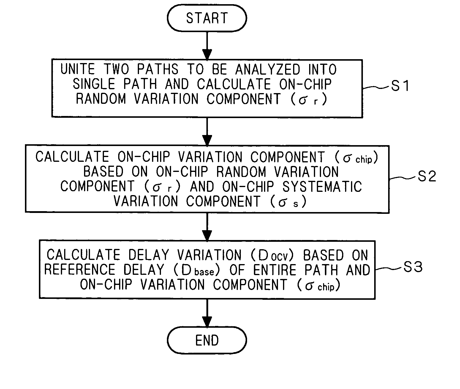
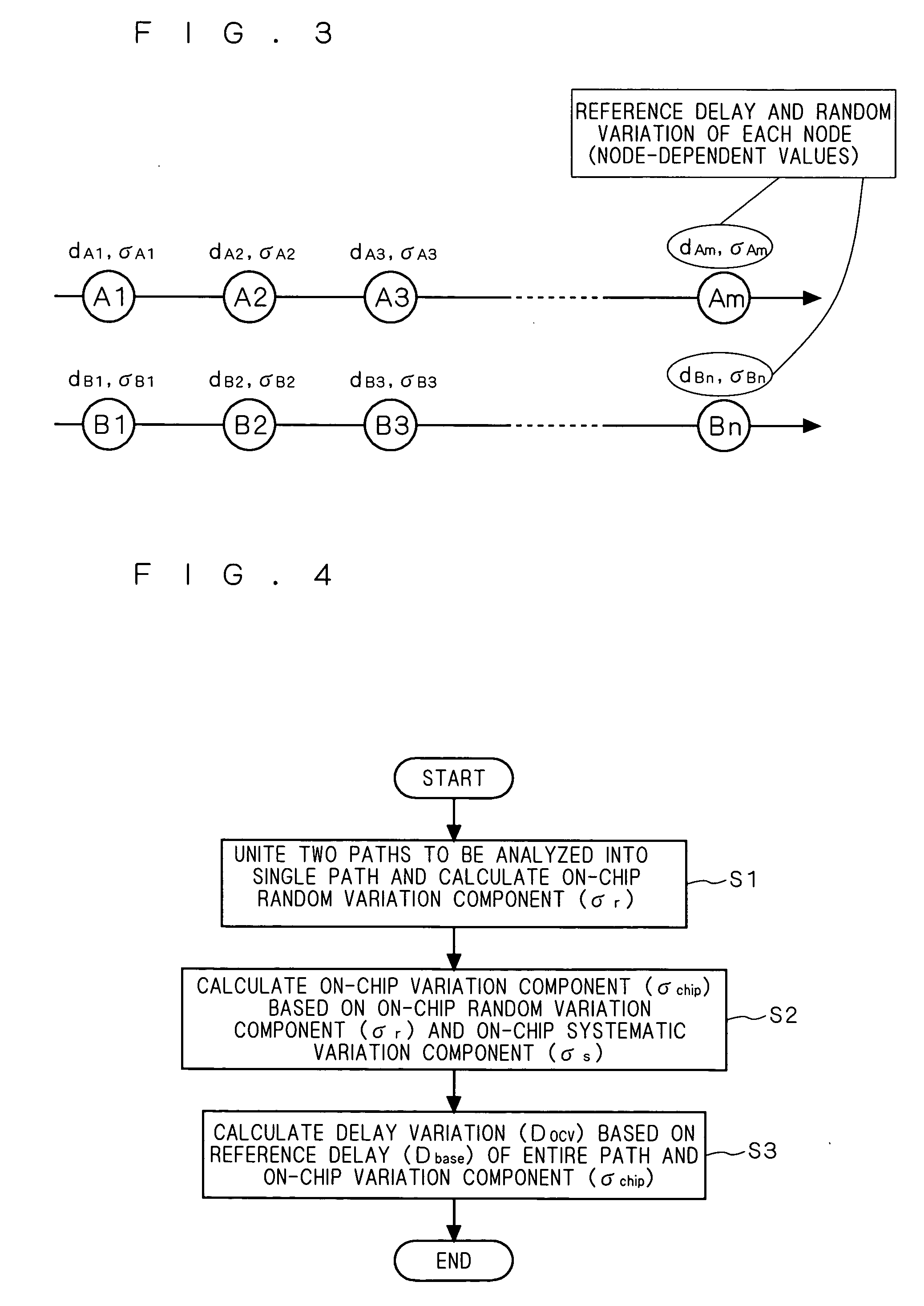
[0035] A. Basic Concept of the Invention

[0036] First, the basic concept of the semiconductor integrated circuit designing method of the invention will be described.

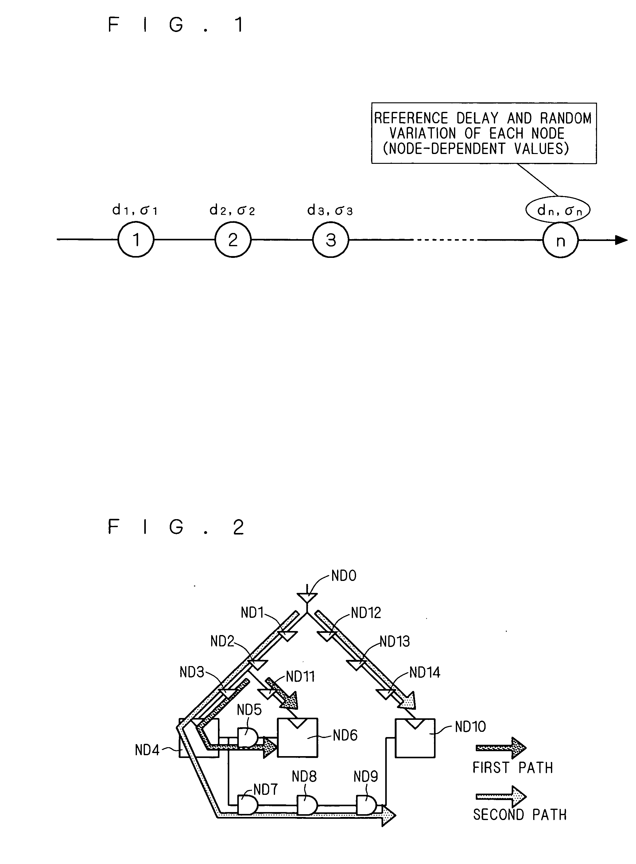
[0037] Components of variations of semiconductor element characteristics caused by semiconductor process are classified, and the ratios of delay variation (deviations from average delay) caused by the variation components are assumed to be normal distributions and represented with standard deviations as described below.

[0038] That is, with a plurality of nodes in a semiconductor chip (hereinafter referred to as “chip”), the standard deviation of random variation components of the nodes is represented as σr, the standard deviation of systematic variation components of the nodes is represented as σs, and the standard deviation of variation components of other chips (Off Chip) is represented as σf. Hereinafter, for the sake of convenience, σr, σs, and σf are referred to as a random variation component,...


PUM


Abstract

Two paths (arrival and required paths) as a target of analysis are united into a single path, and an on-chip random variation component σr about a plurality of nodes of the single path is calculated. Next, an on-chip variation component σchip is calculated on the basis of the on-chip random variation component σr and an on-chip systematic variation component σs. Subsequently, a delay variation Docv is calculated on the basis of a reference delay Dbase of the entire path and the on-chip variation component σchip.

Description

BACKGROUND OF THE INVENTION [0001] 1. Field of the Invention [0002] The present invention relates to a method and a program for designing semiconductor integrated circuits and a semiconductor integrated circuit designing apparatus, and particularly to a designing method, a program, and a semiconductor integrated circuit designing apparatus that utilize timing analysis using statistical techniques. [0003] 2. Description of the Background Art [0004]FIG. 11 is a schematic diagram illustrating the concept of Static Timing Analysis (STA) that is known as a method of timing analysis of semiconductor integrated circuits. [0005]FIG. 11 exemplifies a semiconductor integrated circuit having 15 nodes from ND0 to ND14. Nodes are defined herein as elements having delays, such as logic gates and interconnections, and it is assumed that the nodes ND4, ND6, and ND10 are flip-flops, the nodes ND5, ND7 to ND9 are AND logic gates, and the other nodes are unspecified logic gates. [0006] In the static t...

Claims


Application Information

Patent Timeline
IPC IPC(8): G01R29/02G01R35/00
CPCG06F2217/10G06F17/5031G06F30/3312G06F2111/08
Inventor YOSHIKAWA, ATSUSHI
Owner RENESAS ELECTRONICS CORP
Why Eureka
Try Eureka