Thin-film solar cells and photodetectors having enhanced optical absorption and radiation tolerance

a solar cell and film technology, applied in the field of solar cells and photodetectors, can solve the problems of limited application of texturing schemes to thin wafers and films (20-50 m), inability to achieve comparable improvements in silicon solar cells for use in space environments, and loss of significant market share to compound semiconductor multi-junction solar cell technology. achieve enhanced ionizing radiation tolerance, enhanced optical absorption, and enhanced ir respons

a solar cell and film technology, applied in the field of solar cells and photodetectors, can solve the problems of limited application of texturing schemes to thin wafers and films (20-50 m), inability to achieve comparable improvements in silicon solar cells for use in space environments, and loss of significant market share to compound semiconductor multi-junction solar cell technology. achieve enhanced ionizing radiation tolerance, enhanced optical absorption, and enhanced ir respons

US20070084505A1Inactive Publication Date: 2007-04-19ZAIDI SALEEM H

Image

  • Thin-film solar cells and photodetectors having enhanced optical absorption and radiation tolerance
  • Thin-film solar cells and photodetectors having enhanced optical absorption and radiation tolerance
  • Thin-film solar cells and photodetectors having enhanced optical absorption and radiation tolerance

Examples


Embodiment Construction

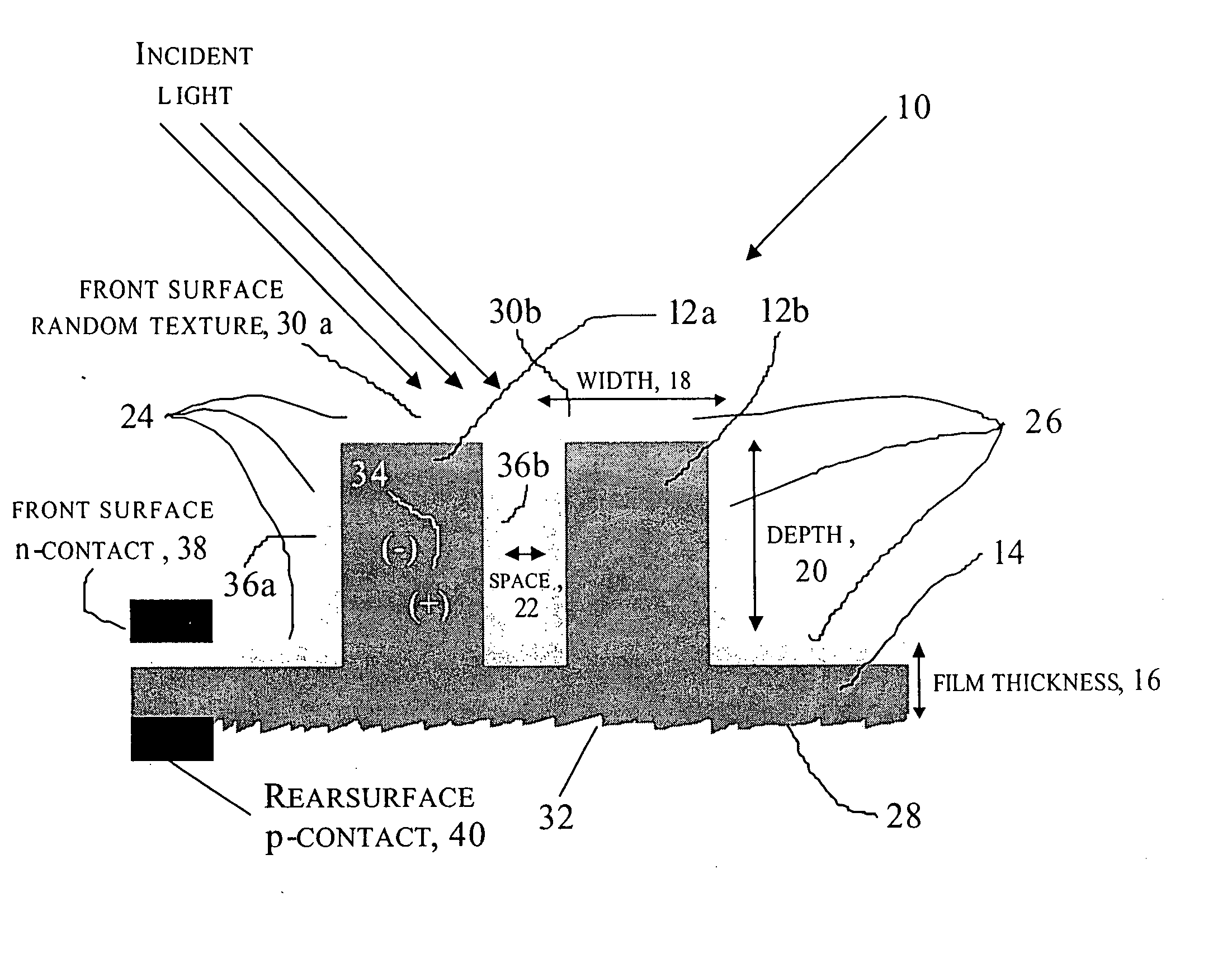
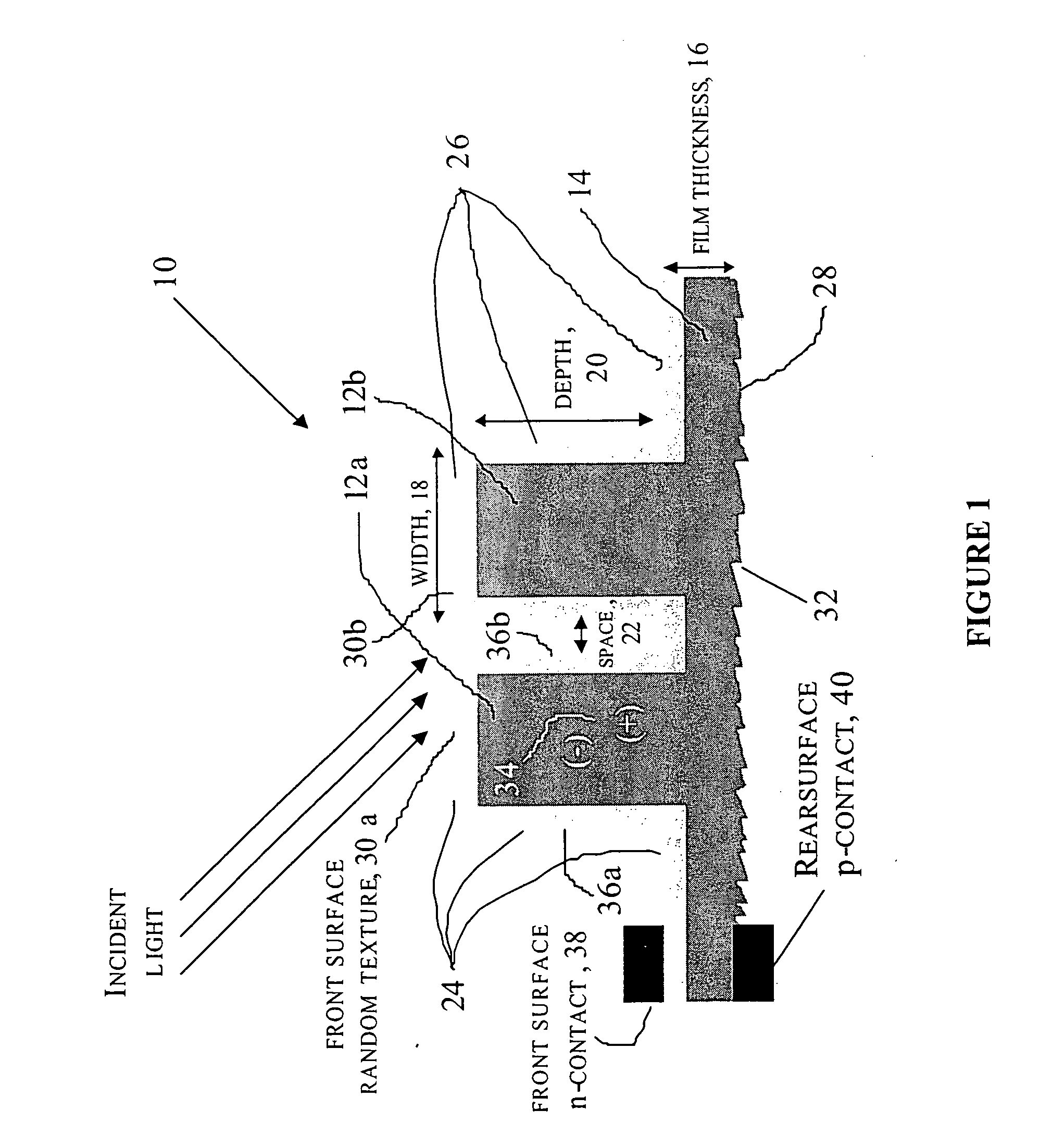
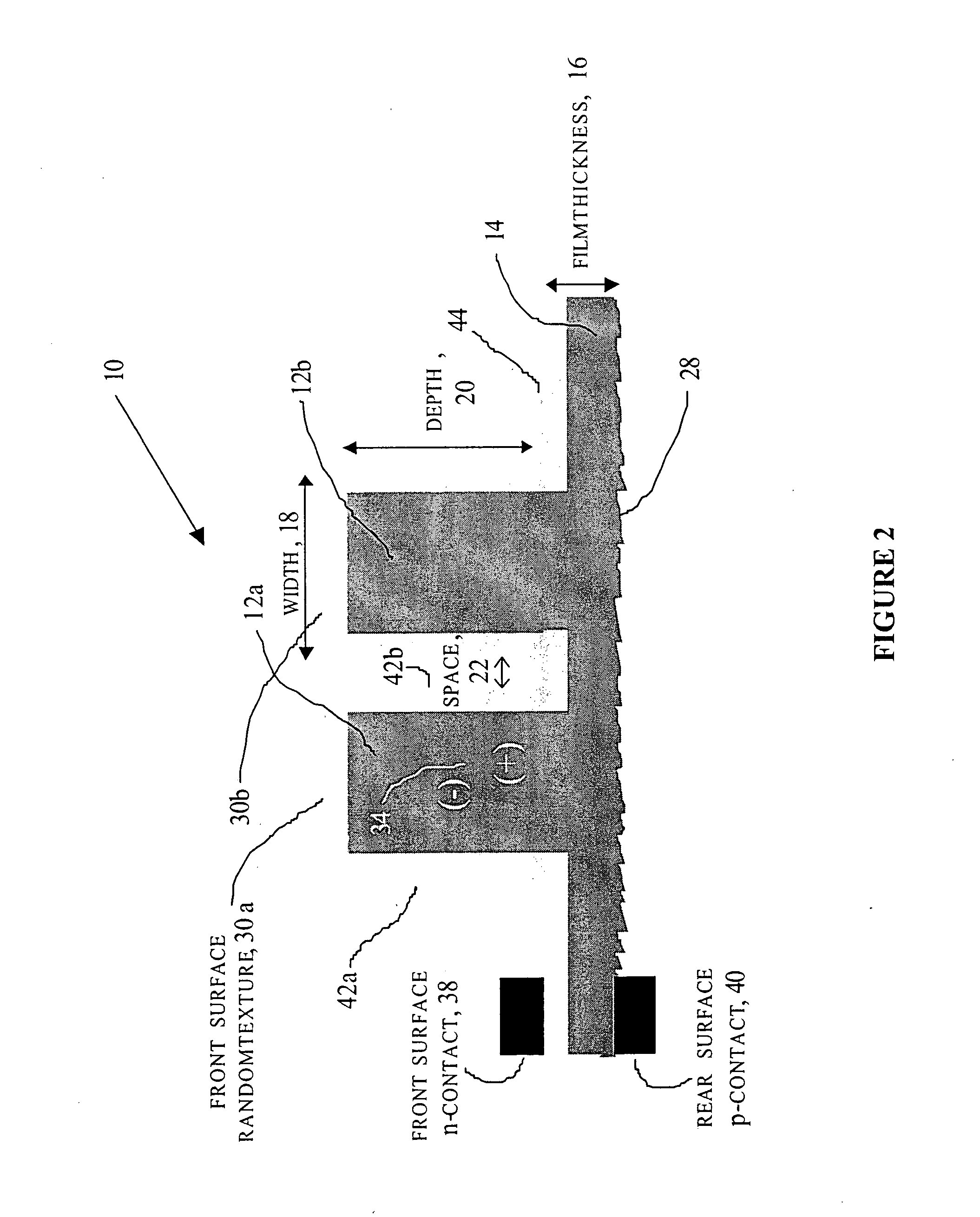
[0047] Briefly, the present invention includes the use of subwavelength random and periodic microscopic structures for enhancing light absorption and immunity to ionizing radiation damage of thin-film solar cells and photodetectors, hereinafter being referred to as photovoltaic devices. Front surface random and periodic microscopic structures can be classified either as diffractive or waveguide elements. Diffractive front surface microscopic structures scatter light into oblique propagating higher diffraction orders that are effectively trapped within periodic surface features etched through the majority of the thin film. The microscopic periodic surface features further enhance absorption by acting as light waveguides perpendicular to the solar cell surface. Typically, the photovoltaic devices of the present invention have dimensions as follows: thin film thickness is between 15 μm and 50 μm, and the plurality of surface features each have a chosen width between 1 μm and 50 μm, a d...


PUM


Abstract

Subwavelength random and periodic microscopic structures are used to enhance light absorption and tolerance for ionizing radiation damage of thin film and photodetectors. Diffractive front surface microscopic structures scatter light into oblique propagating higher diffraction orders that are effectively trapped within the volume of the photovoltaic material. For subwavelength periodic microscopic structures etched through the majority of the material, enhanced absorption is due to waveguide effect perpendicular to the surface thereof. Enhanced radiation tolerance of the structures of the present invention is due to closely spaced, vertical sidewall junctions that capture a majority of deeply generated electron-hole pairs before they are lost to recombination. The separation of these vertical sidewall junctions is much smaller than the minority carrier diffusion lengths even after radiation-induced degradation. The effective light trapping of the structures of the invention compensates for the significant removal of photovoltaic material and substantially reduces the weight thereof for space applications.

Description

RELATED CASES [0001] The present patent application claims the benefit of Provisional Patent Application Ser. No. 60 / 332,777 filed on Nov. 16, 2001 for “Method Of Deeply Etched Subwavelength Structures For Enhanced Optical Absorption In Solar Cells And Photodetectors.”STATEMENT REGARDING FEDERAL RIGHTS [0002] This invention was made in part with government support under Contract No. F29601-00-C-0158 between the U.S. Missile Defense Agency and Gratings Incorporated, a New Mexico corporation. The government has certain rights in the invention.FIELD OF THE INVENTION [0003] The present invention relates generally to solar cells and photodetectors and, more particularly, to enhancement of absorption and tolerance to ionizing radiation, resulting from surface random and periodic microstructures formed from the material of the solar cell or photodetector for thin film (<50 μm) solar cells and photodetectors. BACKGROUND OF THE INVENTION [0004] Since its inception more than fifty years ag...

Claims


Application Information

Patent Timeline
19 Apr 2007
Publication
US20070084505A1
IPC
H01L31/00; H01J40/14
CPC
H01L31/035281; H01L31/03529; H01L31/03921; H01L31/1804; H01L31/02363; Y02E10/547; Y02P70/50
Inventors
ZAIDI, SALEEM H.