Light-emitting diode and method for manufacturing same, integrated light-emitting diode and method for manufacturing same, method for growing a nitride-based iii-v group compound semiconductor, substrate for growing a nitride-based iii-v group compound semiconductor, light source cell unit, light-emitting diode backlight, light-emitting diode illuminating device, light-emitting diode display and electronic instrument, electronic device and method for manufacturing same

a technology of light-emitting diodes and manufacturing methods, which is applied in the direction of chemically reactive gas growth, polycrystalline material growth, and growth of polycrystalline materials. it can solve the problems of affecting the etching process. it can achieve the effect of improving the light extraction efficiency and reducing the luminous efficiency of the light-emitting diodes

Inactive Publication Date: 2007-04-19
SONY CORP
View PDF12 Cites 131 Cited by
  • Summary
  • Abstract
  • Description
  • Claims
  • Application Information

AI Technical Summary

Benefits of technology

[0014] With the conventional method illustrated with respect to FIGS. 77A to 77C, the formation of the space 103 between the sapphire substrate 101 and the GaN semiconductor layer 102 is as stated hereinabove. According to the results of a test made by us, where a light-emitting diode structure in which a GaN semiconductor layer is formed on the GaN semiconductor layer 102 is formed, there is left a problem that the luminous efficiency of the light-emitting diode is low. This is considered for the reason that light generated from an active layer in the course of operation of the light-emitting diode is repeatedly reflected at the inside of the space 103 and is eventually absorbed, thereby worsening a light extraction efficiency.

Problems solved by technology

According to the results of a test made by us, where a light-emitting diode structure in which a GaN semiconductor layer is formed on the GaN semiconductor layer 102 is formed, there is left a problem that the luminous efficiency of the light-emitting diode is low.
This is considered for the reason that light generated from an active layer in the course of operation of the light-emitting diode is repeatedly reflected at the inside of the space 103 and is eventually absorbed, thereby worsening a light extraction efficiency.
Further, in either of the conventional growth methods illustrated in FIGS. 77A to 77C and 80A to 80F, dry etching is usually used to subject the surface of the sapphire substrate 101 to patterned indentation, but the sapphire substrate 101 is very unlikely to undergo dry etching, thus not only taking a long time for the etching, but also being low in processing accuracy.

Method used


Image

  • Light-emitting diode and method for manufacturing same, integrated light-emitting diode and method for manufacturing same, method for growing a nitride-based iii-v group compound semiconductor, substrate for growing a nitride-based iii-v group compound semiconductor, light source cell unit, light-emitting diode backlight, light-emitting diode illuminating device, light-emitting diode display and electronic instrument, electronic device and method for manufacturing same
  • Light-emitting diode and method for manufacturing same, integrated light-emitting diode and method for manufacturing same, method for growing a nitride-based iii-v group compound semiconductor, substrate for growing a nitride-based iii-v group compound semiconductor, light source cell unit, light-emitting diode backlight, light-emitting diode illuminating device, light-emitting diode display and electronic instrument, electronic device and method for manufacturing same
  • Light-emitting diode and method for manufacturing same, integrated light-emitting diode and method for manufacturing same, method for growing a nitride-based iii-v group compound semiconductor, substrate for growing a nitride-based iii-v group compound semiconductor, light source cell unit, light-emitting diode backlight, light-emitting diode illuminating device, light-emitting diode display and electronic instrument, electronic device and method for manufacturing same

Examples


first embodiment

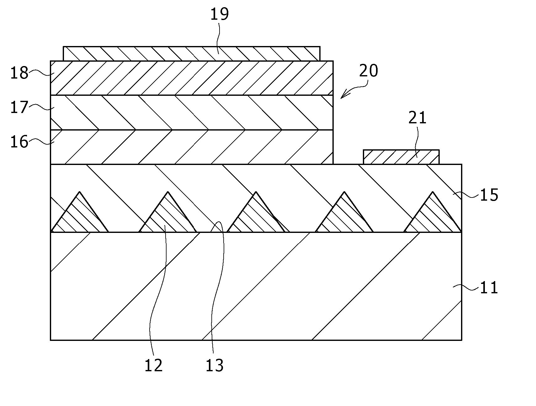
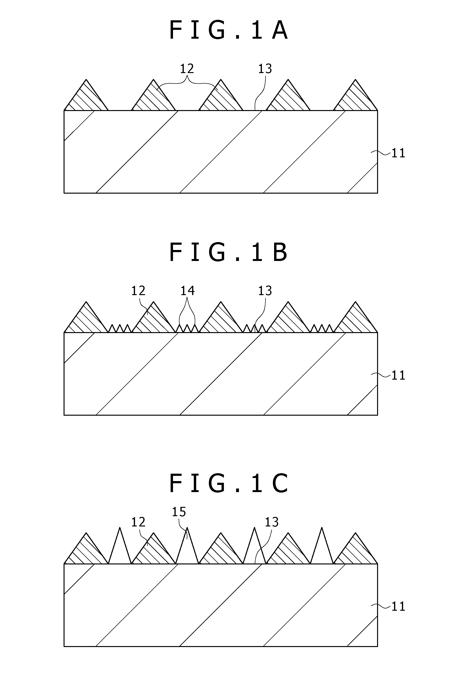
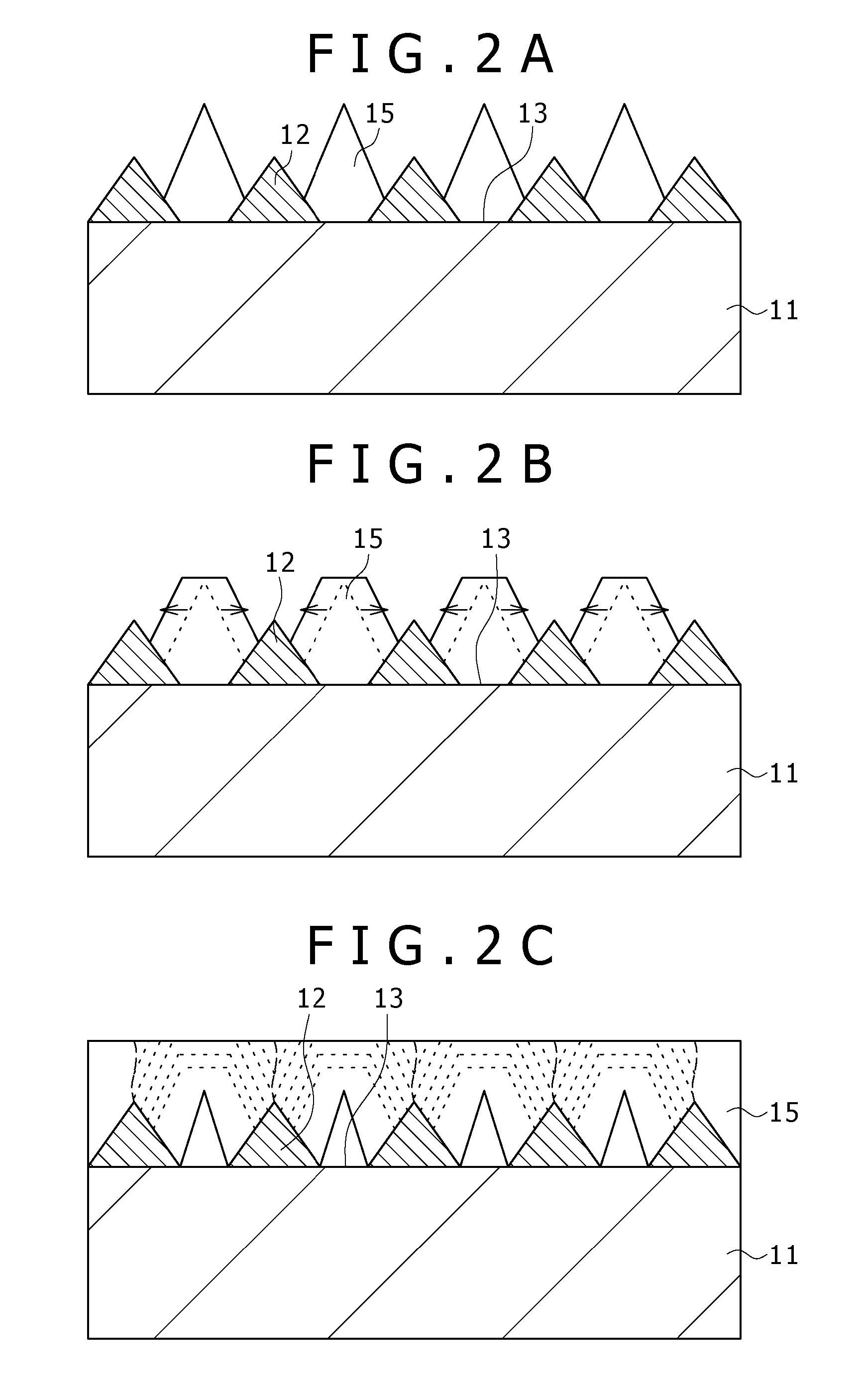
[0148] In FIGS. 1A to 3, a method of manufacturing a light-emitting diode according to the invention is shown in sequence. This light-emitting diode makes use of a nitride-based III-V Group compound semiconductor such as GaN.

[0149] In the first embodiment, as shown in FIG. 1A, a substrate 11 having a flat main surface and made of a material different from a nitride-based III-V compound semiconductor is provided. Protruded portions 12 having a isosceles triangle are formed on the substrate 11 in a given planar pattern at intervals. Thus, a recess 13 having an inverted trapezoid in section is formed between adjacent protruded portions 2. The substrate 11 may be, for example, one that has been stated hereinbefore and includes, for example, a sapphire substrate, with its main face being, for example, a c face. The planar shape or form of the protruded portions 12 and recess portions 13 may be one selected from many planar shapes set out hereinbefore. For instance, the planar shape may b...

second embodiment

[0192] Next, the invention is described.

[0193] In this second embodiment, at the time when the nitride-based III-V Group compound semiconductor layer 15 is grown to an extent of making an isosceles triangle in section using the bottom surface of the recess portion 13 as a base thereof, the height of the protruded portion 12 is so selected that the height of the nitride-based III-V Group compound semiconductor layer 15 is lower than the height of the protruded portion 12. For an instance, the case where the height of the nitride-based III-V Group compound semiconductor layer 15 is equal to the height of the protruded portion 12 is shown in FIGS. 25A and 25B. This leads to the fact that all dislocations, which occur from the interface with the substrate 11 and go through to the side faces of the nitride-based III-V Group compound semiconductor layer 5 having an isosceles triangle in section using the bottom surface of the recess portion 13 as a base thereof, continuedly extend to the ...

third embodiment

[0196] Next, the invention is described.

[0197] In the third embodiment, as shown in FIG. 26, a protruded portion 12 formed on a substrate 11 is shaped in the form of an isosceles triangle in section and in the form of a comb as viewed in plane.

[0198] The third embodiment other than those described above is similar to the first embodiment.

[0199] According to this third embodiment, similar advantages as in the first embodiment can be obtained.


PUM


Abstract

A method for manufacturing a light-emitting diode, which includes the steps of: providing a substrate having a plurality of protruded portions on one main surface thereof wherein the protruded portion is made of a material different in type from that of the substrate and growing a first nitride-based III-V Group compound semiconductor layer on each recess portion of the substrate through a state of making a triangle in section wherein a bottom surface of the recess portion becomes a base of the triangle; laterally growing a second nitride-based III-V Group compound semiconductor layer on the substrate from the first nitride-based III-V Group compound semiconductor layer; and successively growing, on the second nitride-based III-V Group compound semiconductor layer, a third nitride-based III-V Group compound semiconductor layer of a first conduction type, an active layer, and a fourth nitride-based III-V compound semiconductor layer of a second conduction type.

Description

CROSS REFERENCES TO RELATED APPLICATIONS [0001] The present application contains subject matter related to Japanese Patent Application JP 2005-275504 filed with the Japanese Patent Office on Sep. 22, 2005, and Japanese Patent Application JP 2006-215342 filed with the Japanese Patent Office on Aug. 8, 2006, the entire contents of which being incorporated herein by reference. BACKGROUND OF THE INVENTION [0002] 1. Field of the Invention [0003] This invention relates to a light-emitting diode and a method for manufacturing same, an integrated light-emitting diode and a method for making same, a method for growing a nitride-based III-V Group compound semiconductor, a substrate for growing a nitride-based III-V Group compound semiconductor, a light source cell unit, a light-emitting diode backlight, a light-emitting diode illuminating device, a light emitting diode display, an electronic instrument, and an electronic device and a method for manufacturing same. The invention is suited for ...

Claims


Application Information

Patent Timeline
Patent Type & Authority Applications(United States)
IPC IPC(8): H01L33/00H01L21/00H01L33/08H01L33/16H01L33/32
CPCC30B23/04H01L21/0262C30B29/403H01L21/02458H01L21/0254H01L21/02642H01L21/02647H01L33/007H01L33/0079H01L33/08H01L33/12H01L33/22H01L33/46H01L21/02439H01L21/02507C30B25/04H01L33/0093H01L27/15H01L33/0025H01L33/24H01L33/32
Inventor OHMAE, AKIRASHIOMI, MICHINORIFUTAGAWA, NORIYUKIAMI, TAKAAKIMIYAJIMA, TAKAOHIRAMATSU, YUUJIHATADA, IZUHOOKANO, NOBUKATATOMIYA, SHIGETAKAYANASHIMA, KATSUNORIHINO, TOMONORINARUI, HIRONOBU
Owner SONY CORP
Why Eureka
Try Eureka