Display device, method for manufacturing the same, and television apparatus

a technology for television equipment and display devices, which is applied in the field of display devices, can solve the problems of reducing the number of steps, affecting and inevitably increasing the manufacturing cost, and achieves the effects of improving the usability of materials, facilitating the manufacture of steps, and facilitating the use of light exposing equipmen

Active Publication Date: 2007-04-19
SEMICON ENERGY LAB CO LTD
View PDF31 Cites 37 Cited by
  • Summary
  • Abstract
  • Description
  • Claims
  • Application Information

AI Technical Summary

Benefits of technology

[0042] According to the present invention, patterning of a wiring layer and a mask can be directly performed by a droplet discharge method. Therefore, it is

Problems solved by technology

Therefore, as the number of times of the photolithography steps is increased more, a manufacturing cost is inevitably increased more.
However, in the technique disclosed in Reference 1, only some the photolithography steps which are carried out plural times in a TFT manufacturing step a

Method used


Image

  • Display device, method for manufacturing the same, and television apparatus
  • Display device, method for manufacturing the same, and television apparatus
  • Display device, method for manufacturing the same, and television apparatus

Examples


embodiment mode 1

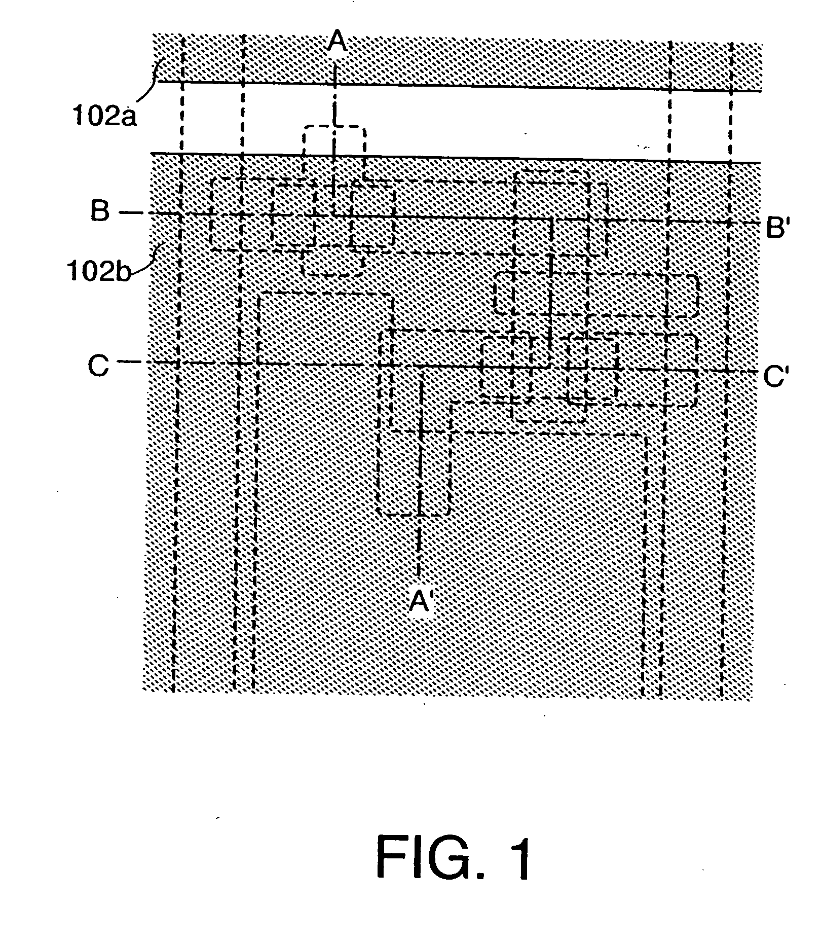
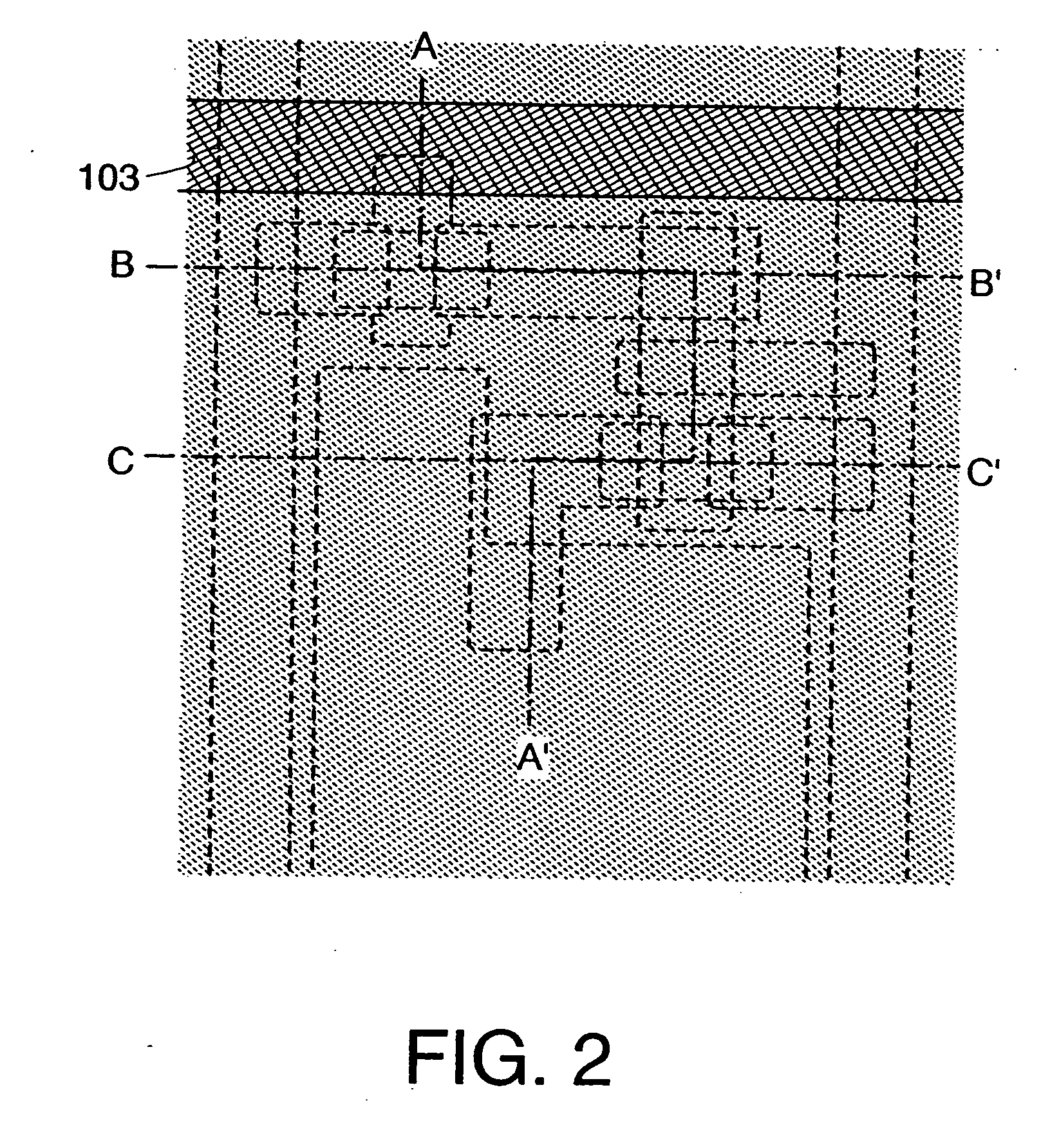
[0106] An embodiment mode of the present invention is described with reference to FIGS. 1 to 7 and FIGS. 16A to 23C. Specifically, a method for manufacturing a display device to which the present invention is applied is described. First, a method for manufacturing a display device having a channel etch thin film transistor to which the present invention is applied is described. FIGS. 1 to 7 correspond to FIGS. 16 to 22, respectively. FIGS. 1 to 7 are top views of a pixel portion of a display device. FIGS. 16A, 17A, 18A, 19A, 20A, 21A, and 22A are cross-sectional views taken along lines A-A′ in FIGS. 1 to 7, and FIGS. 16B, 17B, 18B, 19B, 20B, 21B, and 22B are cross sectional views taken along lines B-B′, and then, FIGS. 16C, 17C, 18C, 19C, 20C, 21C, and 22C are cross-sectional views taken along lines C-C′.

[0107] A base film 101 for improving adhesion is formed over a substrate 100 as base pretreatment. Then, insulating layers 102a and 102b are selectively formed as shown in FIG. 1 a...

embodiment mode 2

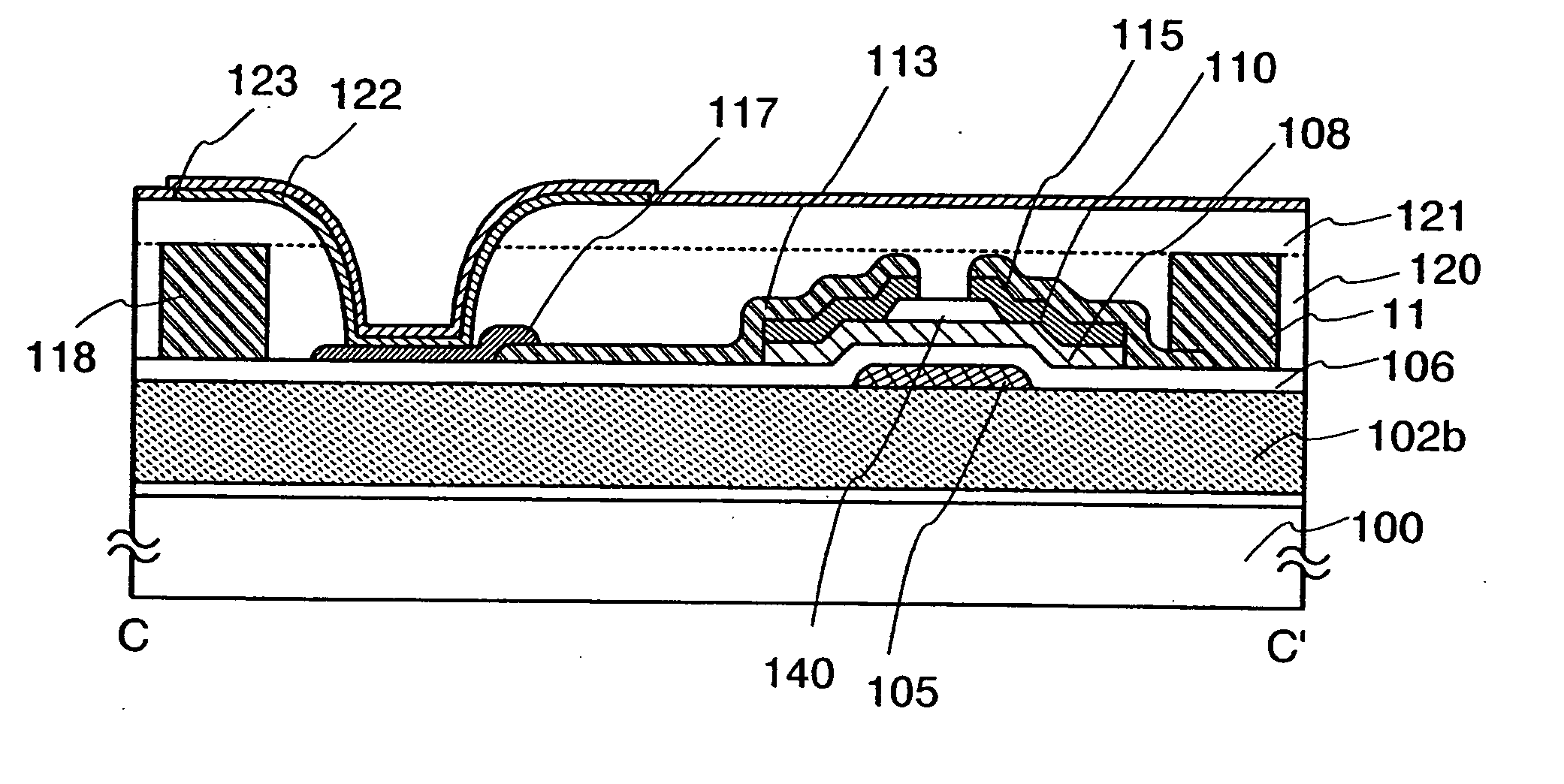
[0172] An embodiment mode of the present invention is described with reference to FIG. 8. This embodiment mode describes the case of using a channel protective thin film transistor as a thin film transistor in Embodiment Mode 1. Therefore, repetitive description of the same portion or a portion having a similar function is omitted. Note that FIG. 8 corresponds to a cross-sectional view of a channel etch thin film transistor in FIG. 23C.

[0173] An insulating layer 102b is formed over a substrate 100, and a gate wiring layer is formed by discharging a composition including a conductive material with a droplet discharge method. A gate electrode layer 105 is formed by a droplet discharge method to be in contact with the gate wiring layer. Subsequently, a gate insulating layer 106 is formed by using a plasma CVD method or a sputtering method to be a single layer or to have a laminated structure. A specifically preferable mode of the gate insulating layer corresponds to a lamination body ...

embodiment mode 3

[0181] This embodiment mode is different from the channel etch type thin film transistor manufactured in Embodiment Mode 1 in a connection structure with a first electrode layer, which is described with reference to FIG. 15.

[0182] Steps up to forming a source-drain electrode layer 113 are similar to those in Embodiment Mode 1. Next, a columnar conductive layer 144 to function as a pillar is formed. In this embodiment mode, conductive layers are laminated using a droplet discharge method to form the columnar conductive layer 144. The columnar conductive layer 144 may be formed either before or after the insulating layer 120 is formed. In the case of forming the insulating layer 120 earlier, a contact hole in which the columnar conductive layer 144 is to be formed can be formed together with an interlayer insulating film by selectively forming the insulating layer 120 with a droplet discharge method.

[0183] As another method, a material which repels the insulating layer 120 is discha...


PUM


Abstract

An object of the present invention is to provide a display device which can be manufactured with usability of a material improved and with a manufacturing step simplified and to provide a manufacturing technique thereof. One feature of a display device of the present invention is to comprise an insulating layer having an opening, a first conductive layer formed in the opening, and a second conductive layer formed over the insulating layer and the first conductive layer, wherein the first conductive layer is wider and thicker than the second conductive layer, and the second conductive layer is formed by spraying a droplet including a conductive material.

Description

TECHNICAL FIELD [0001] The present invention relates to a display device employing a droplet discharge method and to a manufacturing method thereof. BACKGROUND ART [0002] A thin film transistor (hereinafter, referred to as a “TFT”) and an electronic circuit using the thin film transistor are manufactured by laminating various thin films of a semiconductor, an insulating material, a conductive material, and the like over a substrate and then appropriately forming a predetermined pattern with a photolithography technique. The photolithography technique means a technique of transferring a pattern of a circuit or the like formed over a surface of a transparent flat plane referred to as a photomask by using a material which does not transmit light onto a targeted substrate by utilizing light, and the technique has been widely used in a manufacturing step of a semiconductor integrated circuit or the like. [0003] In a manufacturing step employing a conventional photolithography technique, ...

Claims


Application Information

Patent Timeline
IPC IPC(8): G02F1/136H01L29/04H01L21/84H01L29/10H01L21/00H01L31/00G09F9/30H01L21/77H01L27/12H01L27/32
CPCH01L27/12H01L27/1292H01L27/124H01L27/3262H10K59/1213H01L21/288H01L27/1214H01L27/1218H01L29/41733H01L29/42384
Inventor YAMAZAKI, SHUNPEIKUWABARA, HIDEAKIMAEKAWA, SHINJIFUJII, GENISA, TOSHIYUKI
Owner SEMICON ENERGY LAB CO LTD
Why Eureka
Try Eureka