Coated nano particle and electronic device using the same

a nano-particle and electronic device technology, applied in the field of nano-particles, can solve the problems of reducing luminous efficiency and deteriorating absorption efficiency of optical energy, and achieve the effect of minimizing light loss and improving luminous efficiency

Active Publication Date: 2007-04-19
SAMSUNG ELECTRONICS CO LTD
View PDF16 Cites 55 Cited by
  • Summary
  • Abstract
  • Description
  • Claims
  • Application Information

AI Technical Summary

Benefits of technology

[0010] The present invention may provide a coated nano particle and an electronic device including the coated nano particle for improving the luminous efficiency by minimizing lost light which is scattered or reabsorbed at an interface by coating the surface of a nano particle used as an illuminator with a material having a lower index of refraction than that of the nano particle.

Problems solved by technology

That is, since light scattering occurs at the interface between the matrix and the illuminator due to the difference between an index of refraction of the matrix Nm and an index of refraction of the illuminator Np, the absorption efficiency of the optical energy is deteriorated, and the light emitted from the illuminator is reflected from the interface between the matrix and the illuminator, and is reabsorbed by the illuminator, thereby decreasing the luminous efficiency.

Method used


Image

  • Coated nano particle and electronic device using the same
  • Coated nano particle and electronic device using the same
  • Coated nano particle and electronic device using the same

Examples


embodiment 1

CdSeS Nano Particle Compound With Pyridine Replaced

[0072] 16 g of trioctylamine (TOA), 0.5 g of oleic acid, and 0.4 mmol of cadmium oxide are put into a 125 ml flask having a reflux condenser, and are agitated while controlling a reaction temperature at 300° C. In the meantime, Se powder is dissolved in trioctylphosphine (TOP) so as to make a Se-TOP complex solution having a Se concentration of about 0.25 M. S powder is dissolved in TOP so as to make a S-TOP complex solution having a S concentration of about 1.0 M. 0.9 ml of the S-TOP complex solution and 0.1 ml of the Se-TOP complex solution are quickly injected into the reaction mixture including cadmium, and are agitated for 4 minutes. When the reaction is completed, after decreasing a temperature of the reaction mixture rapidly if possible, and adding ethanol as non-solvent, centrifugation is performed. An upper portion of the solution lacking the centrifugal precipitate is withdrawn, and the precipitate is dispersed to toluen...

embodiment 2

CdSeS Nano Crystal Coated With SiO2 and With Pyridine Replaced

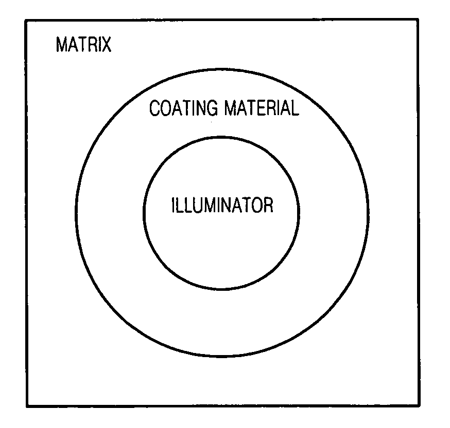
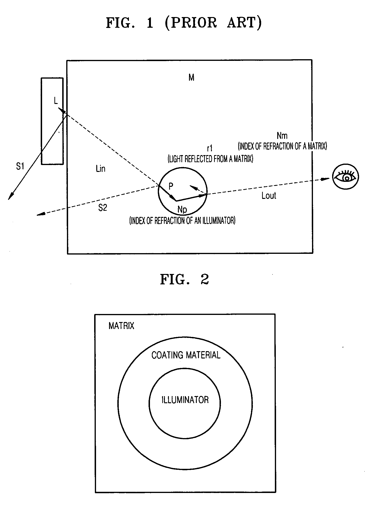
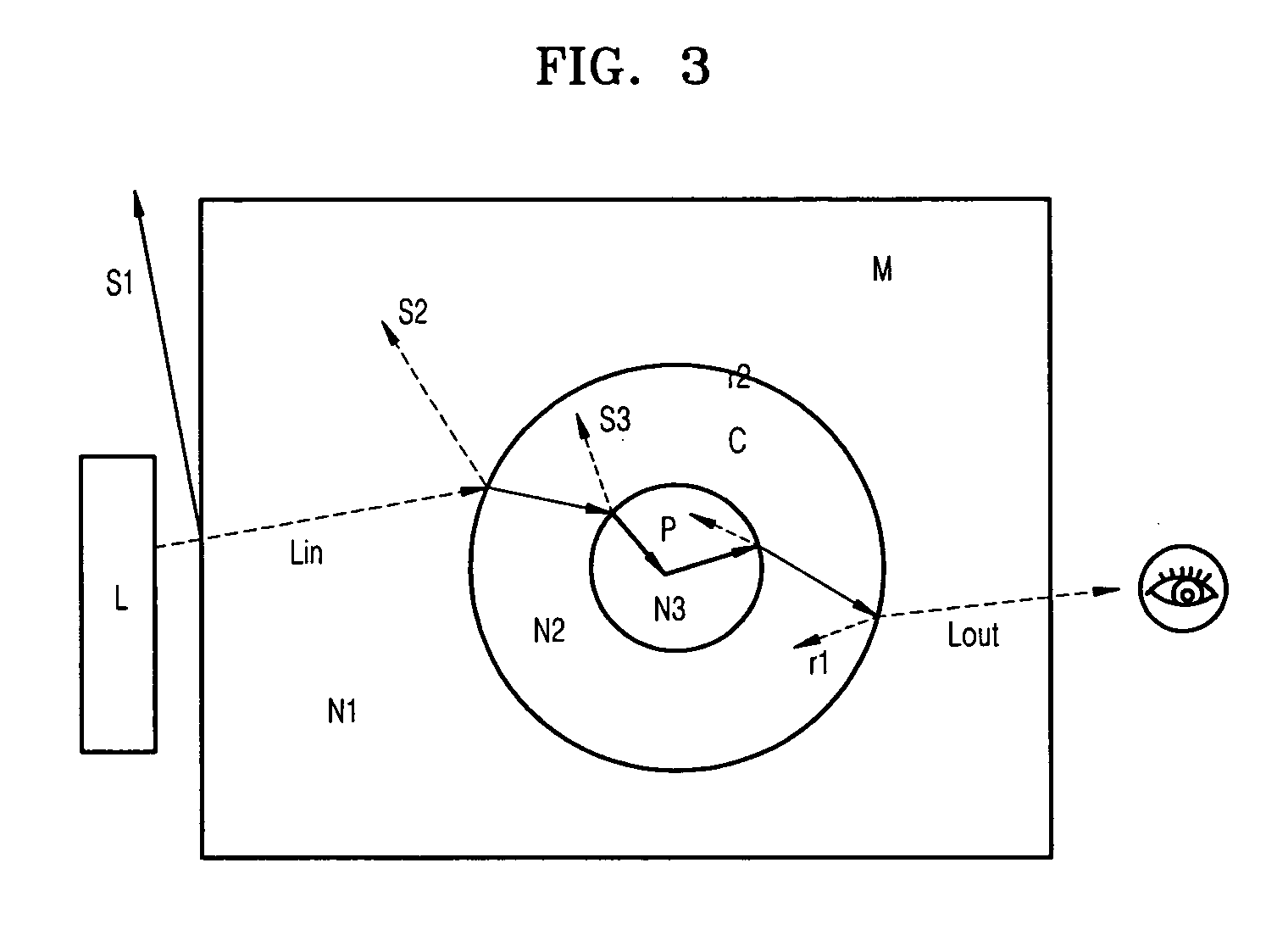
[0075] Ethanol as non-solvent is added to the toluene solution of the CdSeS nano particle fabricated in the Embodiment 1, and centrifugation is performed. An upper portion of the solution except for the centrifugal precipitate is drawn, and the precipitate is dispersed to pyridine and is agitated for about 30 minutes. After agitating, hexane as non-solvent is added and centrifugation is performed. The centrifugal precipitate is dispersed to pyridine again, and 0.1 ml of triethoxy silane (TEOS) is added, and is agitated for about 3 hours at a room temperature so as to form a SiO2 layer on a surface of CdSeS. After agitating, hexane as non-solvent is added, and centrifugation is performed. Thereafter an upper portion of the solution lacking the centrifugal precipitate is withdrawn, and the precipitate is dispersed to butanol (1.4 of index of refraction) to form an about 1 wt % of solution. A light absorbing spectrum and a...


PUM

PropertyMeasurementUnit
wavelengthaaaaaaaaaa
thicknessaaaaaaaaaa
temperatureaaaaaaaaaa

Abstract

A coated nano particle and an electronic device using the composite nano particle as an illuminator are provided. The composite nano particle includes a nano particle receiving light and emitting light; and a coating material formed on a surface of the nano particle and having an index of refraction different from that of the nano particle. The coated nano particle is made by coating a surface of the nano particle with a material having an index of refraction, which has an intermediate value between an index of refraction of a matrix and an index of refraction of the nano particle as an illuminator, with a predetermined thickness. The light emitted from the nano particle is efficiently transferred to the outside as the light reflected from the matrix and absorbed by the nano particle is suppressed. Therefore, a luminous efficiency of the illuminator is improved, and an electronic device using the illuminator is provided.

Description

CROSS-REFERENCE TO RELATED PATENT APPLICATION [0001] This application claims the benefit of Korean Patent Application No. 10-2005-0040675, filed on May 16, 2005, in the Korean Intellectual Property Office, the disclosure of which is incorporated herein in its entirety by reference. BACKGROUND OF THE DISCLOSURE [0002] 1. Field of the Disclosure [0003] The present disclosure relates to a nano particle used as an illuminator in an electronic device, and more particularly, to a nano particle coated with a material having a lower index of refraction than that of the nano particle on the surface of the nano particle, for improving the luminous efficiency of the electronic device. [0004] 2. Description of the Related Art [0005] Recently, many attempts have been made to employ a nano particle as an illuminator of an electronic device. Among the nano particles, a quantum dot (QD) as a compound semiconductor nano particle is being actively investigated. [0006] The quantum dot is a semiconduct...

Claims


Application Information

Patent Timeline
Patent Type & Authority Applications(United States)
IPC IPC(8): B32B5/16H01L33/44H01L33/50H01L33/62
CPCB82Y20/00Y10T428/256C01B19/002C01B19/007C01P2002/85C01P2004/04C01P2004/64C01P2004/80C01P2006/60C09K11/025C09K11/883Y10T428/2998Y10T428/2991Y10T428/24942B82Y30/00
Inventor JANG, EUN-JOOJUN, SHIN-AE
Owner SAMSUNG ELECTRONICS CO LTD
Why Eureka
Try Eureka