Semiconductor device and manufacturing method thereof

a technology of semiconductors and manufacturing methods, applied in the direction of solid-state devices, contact members penetrating/cutting insulation/cable strands, basic electric elements, etc., can solve problems such as whole defect, and achieve the effect of low wires and no increase in manufacturing steps

Inactive Publication Date: 2007-04-19
SEMICON ENERGY LAB CO LTD
View PDF19 Cites 22 Cited by
  • Summary
  • Abstract
  • Description
  • Claims
  • Application Information

AI Technical Summary

Benefits of technology

[0037] In addition, conventionally a wire is formed to be wide in a contact hole forming portion. However, in the present invention, the first layer is formed to be wide without increasing the number of steps, so that the wire does not require an additional step to be widened. In a contact hole forming portion, an edge of the first wire is projected from an edge of the second wire, thereby forming the first wire longer than the second wire.
[0038] The present invention uses a photo mask or a reticle each of which is provided with a diffraction grating pattern or with an auxiliary pattern formed of a semi-translucent film having a light intensity reducing function, and therefore, the lower wire can be manufactured without increasing the number of manufacturing steps.

Problems solved by technology

In an integrated circuit, one breaking causes a whole defect.
Therefore, it is an important challenge to reduce breaking.

Method used


Image

  • Semiconductor device and manufacturing method thereof
  • Semiconductor device and manufacturing method thereof
  • Semiconductor device and manufacturing method thereof

Examples


embodiment mode 1

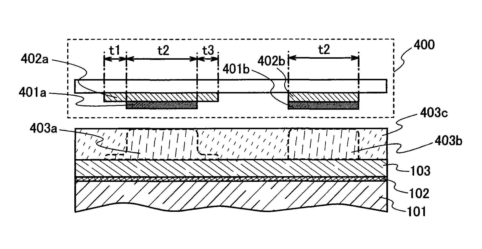
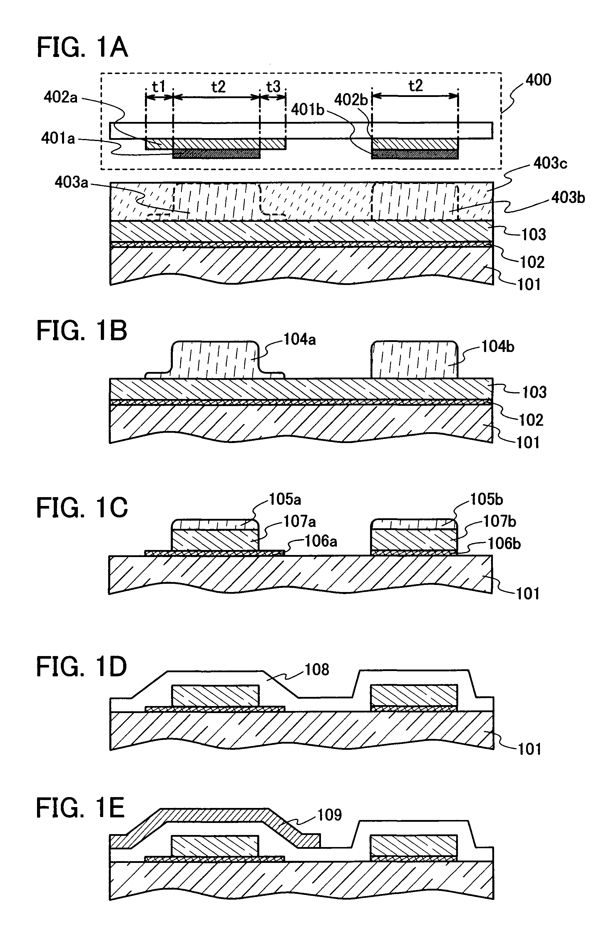
[0052] In this embodiment mode, a manufacturing process for a semiconductor device having a lower wire with a two-layer structure is described. An example of a structure of the semiconductor device, in which the two-layer structured lower wire and an upper wire overlap each other with an insulating film therebetween is described with reference to FIGS. 1A to 1E.

[0053] First, a substrate 101 having an insulating surface is prepared. As the substrate 101 having an insulating surface, a translucent substrate can be used, such as a glass substrate, a crystallized glass substrate, or a plastic substrate. Besides, as long as the substrate 101 having an insulating surface has an insulating surface as the outermost layer or film, the substrate 101 having the insulating surface may be provided with a base film formed of an insulator, a semiconductor layer, or a conductive film.

[0054] Next, a first conductive layer 102 is formed over the substrate 101 having an insulating surface and a seco...

embodiment mode 2

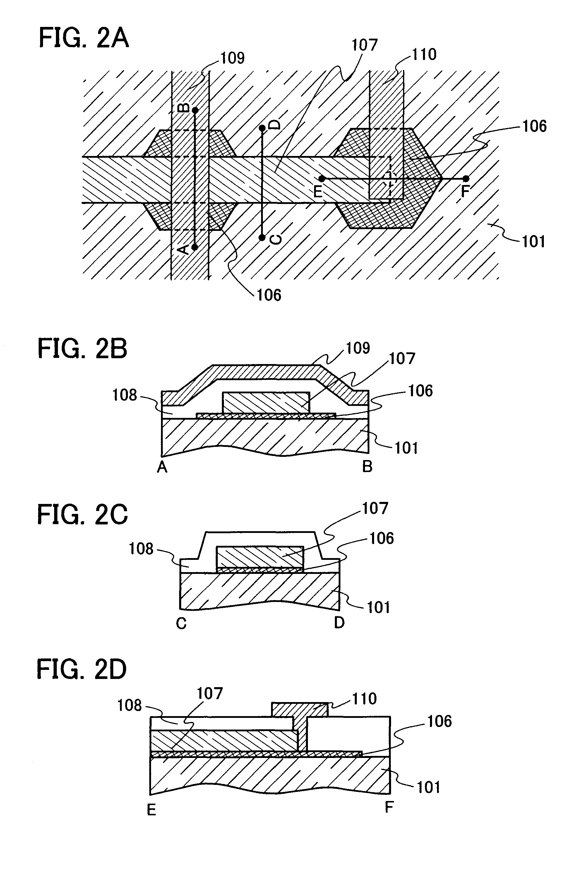
[0068] In this embodiment mode, another structure of Embodiment Mode 1 is described with reference to FIGS. 11A to 11E.

[0069] First, the substrate 101 having an insulating surface is prepared as shown in FIG. 11A. As the substrate 101 having an insulating surface, a translucent substrate can be used, such as a glass substrate, a crystallized glass substrate, or a plastic substrate. Besides, as long as the substrate 101 having an insulating surface has an insulating surface as the outermost layer or film, the substrate 101 having an insulating surface may be provided with a base film formed of an insulator, a semiconductor layer, or a conductive film.

[0070] Next, the first conductive layer 102 is formed over the substrate 101 having an insulating surface and the second conductive layer 103 is stacked thereover. The first conductive layer 102 is formed of a high-melting-point metal such as tungsten (W), chromium (Cr), tantalum (Ta), tantalum nitride (TaN), or molybdenum (Mo); or an ...

embodiment mode 3

[0087] In this embodiment mode, a light exposure mask which is different from those of Embodiment Modes 1 and 2 is described with reference to FIGS. 12A to 12D.

[0088] In this embodiment mode, a light exposure mask including a semi-translucent portion formed by lines (also called non-opening portion) and spaces (also called opening portion), or rectangular patterns and spaces is explained with reference to FIGS. 12A to 12D.

[0089] Specific examples of top views of light exposure masks are shown in FIGS. 12A to 12C. In addition, an example of light intensity distribution when using the light exposure mask is shown in FIG. 12D. Each of the light exposure masks shown in FIGS. 12A to 12C includes a light shielding portion P, a semi-translucent portion Q, and a translucent portion R. In the semi-translucent portion Q of the light exposure mask shown in FIG. 12A, lines 303 and spaces 304 are repeatedly provided in stripes (or, in slits), and the lines 303 and the spaces 304 are arranged p...


PUM


Abstract

It is an object of the present invention to provide a method for preventing a breaking and poor contact, without increasing the number of steps, thereby forming an integrated circuit with high driving performance and reliability. The present invention applies a photo mask or a reticle each of which is provided with a diffraction grating pattern or with an auxiliary pattern formed of a semi-translucent film having a light intensity reducing function to a photolithography step for forming wires in an overlapping portion of wires. And a conductive film to serve as a lower wire of a two-layer structure is formed, and then, a resist pattern is formed so that a first layer of the lower wire and a second layer narrower than the first layer are formed for relieving a steep step.

Description

BACKGROUND OF THE INVENTION [0001] 1. Field of the Invention [0002] The present invention relates to a semiconductor device including a circuit including a semiconductor element and a manufacturing method thereof. In addition, the present invention relates to an electronic appliance to which a light emitting display device including an organic light emitting element or an electro-optic device typified by a liquid crystal display panel is mounted as a part component. Note that in this specification, a semiconductor device refers to a device in general which functions by utilizing semiconductor characteristics. Electro-optic devices, semiconductor circuits, and electronic appliances are all semiconductor devices. [0003] 2. Description of the Related Art [0004] Conventionally, a structure is widely known where thin film transistors (also referred to as TFTs) are integrated to be utilized, in the case where a circuit in an active matrix liquid crystal display device, an image sensor, or...

Claims


Application Information

Patent Timeline
Patent Type & Authority Applications(United States)
IPC IPC(8): H01R4/24
CPCH01L27/1214H01L27/3276H01L27/1288H01L21/76816H01L21/76879H01L23/528H01L2924/0002H01L27/1244H01L27/1259H01L27/124H01L2924/00H10K59/131H01L21/32139H01L21/76834H01L21/76886H01L27/1222H01L27/1274
Inventor SAKAKURA, MASAYUKIOHNUMA, HIDETOKUWABARA, HIDEAKI
Owner SEMICON ENERGY LAB CO LTD
Why Eureka
Try Eureka