Etching processes using c4f8 for silicon dioxide

a silicon dioxide and etching process technology, applied in the field of semiconductor fabrication, can solve the problems of reducing the etching rate, and reducing the conventional rie process for removing tin from the dielectric etching tool, so as to reduce the esd d

Inactive Publication Date: 2007-05-03
GOOGLE LLC
View PDF16 Cites 12 Cited by
  • Summary
  • Abstract
  • Description
  • Claims
  • Application Information

AI Technical Summary

Benefits of technology

[0009] The invention includes methods of etching a dielectric layer and a cap layer over a conductor to expose the conductor. In one embodiment, the methods include the use of a silicon dioxide (SiO2) etchi...

Problems solved by technology

The conventional RIE process for removing TiN in a dielectric etch tool suffers from a number of problems.
First, it leads to tool degradation, and more specifically, to a lowered etch rate and a decreased etch uniformity of subsequent RIE processing, which reduces yield.
Second, typical plasma proc...

Method used


Image

  • Etching processes using c4f8 for silicon dioxide
  • Etching processes using c4f8 for silicon dioxide
  • Etching processes using c4f8 for silicon dioxide

Examples


Embodiment Construction

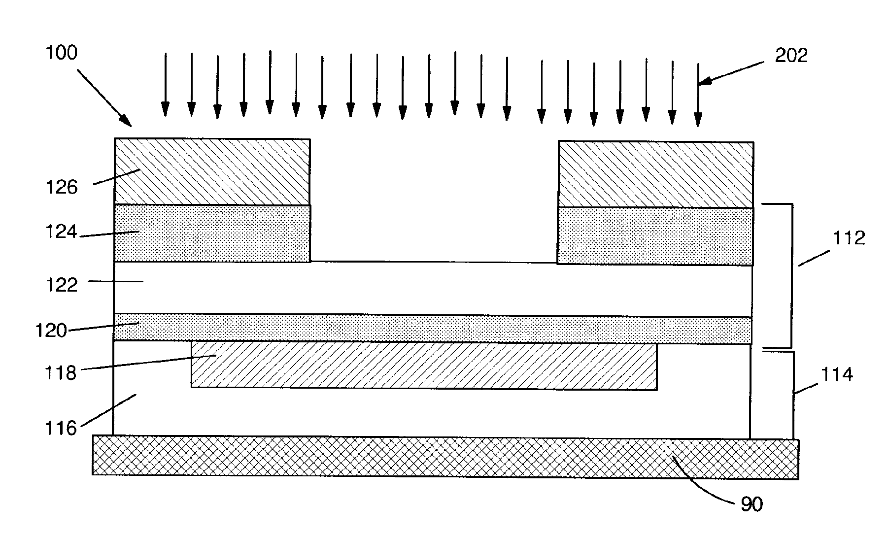
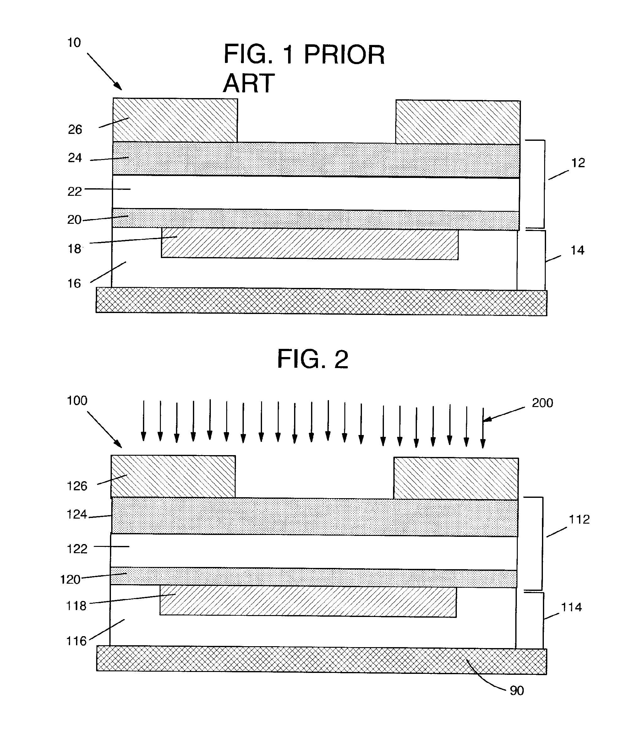
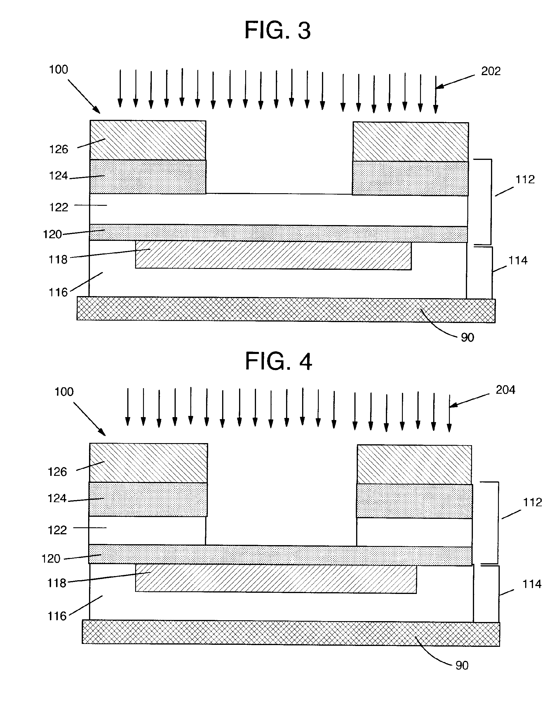
[0018] With reference to the accompanying drawings, FIG. 2-6 show one embodiment of a method of etching to form an opening to expose a conductor according to the invention. A pattern for the opening is provided by a photoresist. The method modifies the conventional process such that electro-static discharge (ESD) defects are reduced and etch rates are not degraded. The process is carried out in a typical dielectric reactive ion etching (RIE) tool, i.e., not a metal RIE tool. The RIE chamber used is capable of two RF settings, e.g., approximately 2 MHz (bottom RF source electrode) and approximately 27 MHz (top bias power electrode).

[0019] The process begins with a conventional semiconductor structure 100 including a stack (sometimes referred to as a large-via pad stack) including dielectric layers 112, similar to that shown in FIG. 1. Structure 100 includes a conductor level 114 including a dielectric layer 116 (e.g., of silicon dioxide (SiO2) or any other appropriate dielectric mat...


PUM

PropertyMeasurementUnit
Temperatureaaaaaaaaaa
Pressureaaaaaaaaaa
Pressureaaaaaaaaaa

Abstract

Methods of etching a dielectric layer and a cap layer over a conductor to expose the conductor are disclosed. In one embodiment, the methods include the use of a silicon dioxide (SiO2) etching chemistry including octafluorocyclobutane (C4F8) and a titanium nitride (TiN) etching chemistry including tetrafluoro methane (CF4). The methods prevent etch rate degradation and exhibit reduced electro-static discharge (ESD) defects.

Description

BACKGROUND OF THE INVENTION [0001] 1. Technical Field [0002] The present invention relates generally to semiconductor fabrication, and more particularly, to etching processes using octafluorocyclobutane (C4F8) for silicon dioxide (SiO2) and tetrafluoro methane (CF4) for titanium nitride (TiN). [0003] 2. Related Art [0004] In the semiconductor industry, reactive ion etching (RIE) is used to open pathways for circuitry within a semiconductor chip. One structure formed using RIE, for example, is a via, which electrically connects conductors within different layers. RIE is a variation of plasma (gas) etching in which a semiconductor wafer is placed on a radio frequency (RF) powered electrode, and etching species are extracted and accelerated from the plasma toward the surface to be etched. A chemical etching reaction occurs that removes parts of the surface. RIE is one of the most common etching techniques in semiconductor manufacturing. [0005] Referring to FIG. 1, a conventional semico...

Claims


Application Information

Patent Timeline
IPC IPC(8): C03C25/68H01L21/302B44C1/22H01L21/461
CPCH01L21/31116H01L21/76802
Inventor MEZZAPELLE, JOSEPH J.
Owner GOOGLE LLC
Why Eureka
Try Eureka