Electrically rewritable non-volatile memory element and method of manufacturing the same

a non-volatile memory element, electric rewritable technology, applied in the direction of digital storage, instruments, electrical equipment, etc., can solve the problems of reducing the electrical power consumption of the device, dram is volatile memory that loses stored data, and the limit of the device electrical power consumption can be reduced, so as to improve the heating efficiency and reduce the write current. , the effect of high heating efficiency

Active Publication Date: 2007-05-03
MICRON TECH INC
View PDF13 Cites 51 Cited by
  • Summary
  • Abstract
  • Description
  • Claims
  • Application Information

AI Technical Summary

Benefits of technology

[0024] In accordance with this aspect of the present invention, the top electrode is formed before the recording layer, and the recording layer is formed in the through-hole, resulting in a three-dimensional structure having high heating efficiency.
[0025] As described above, an electrically rewritable non-volatile memory element having improved heating efficiency, and a method of manufacturing the element can be provided. Therefore, not only a write current can be decreased but also a writing speed can be enhanced.

Problems solved by technology

DRAM is volatile memory that loses stored data if its power supply is turned off.
That makes DRAM unsuitable for the storage of programs and archival information.
Also, even when the power supply is turned on, the device has to periodically perform refresh operations in order to retain stored data, so there are limits as to how much device electrical power consumption can be reduced, while yet a further problem is the complexity of the controls run under the controller.
Semiconductor flash memory is high capacity and non-volatile, but requires high current for writing and erasing data, and write and erase times are slow.
These drawbacks make flash memory an unsuitable candidate for replacing DRAM in main memory applications.
There are other non-volatile memory devices, such as magnetoresistive random access memory (MRAM) and. ferroelectric random access memory (FRAM), but they cannot easily achieve the kind of storage capacities that are possible with DRAM.
Since the voltage for inducing the phase change therefore has to be increased, so the structure is not one that is suitable for achieving low-voltage devices.
Thus, it is difficult to adequately raise heating efficiency with devices having a conventional structure.
This makes it difficult to reduce write current, and also makes it difficult to speed up write operations.

Method used


Image

  • Electrically rewritable non-volatile memory element and method of manufacturing the same
  • Electrically rewritable non-volatile memory element and method of manufacturing the same
  • Electrically rewritable non-volatile memory element and method of manufacturing the same

Examples


first embodiment

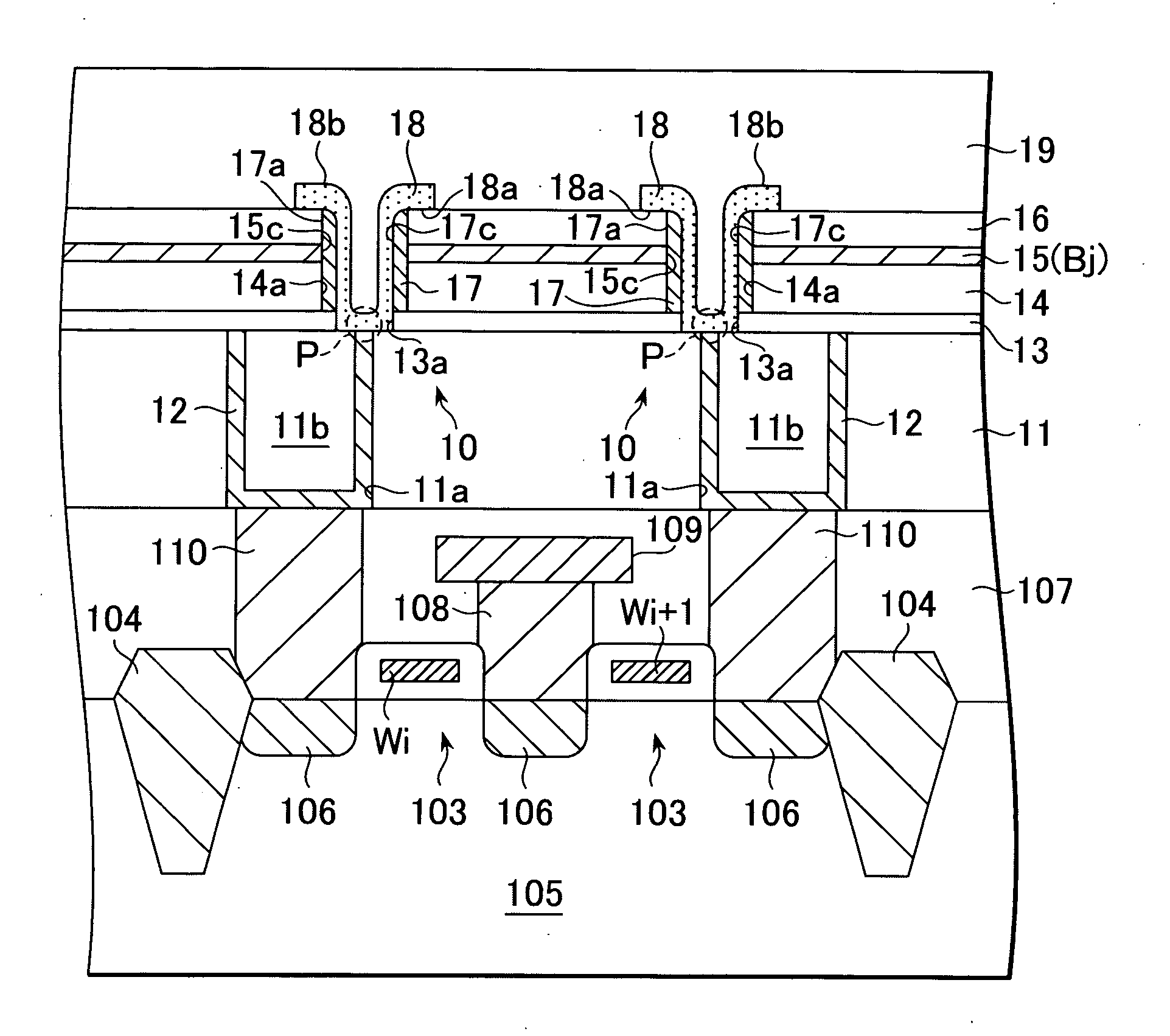
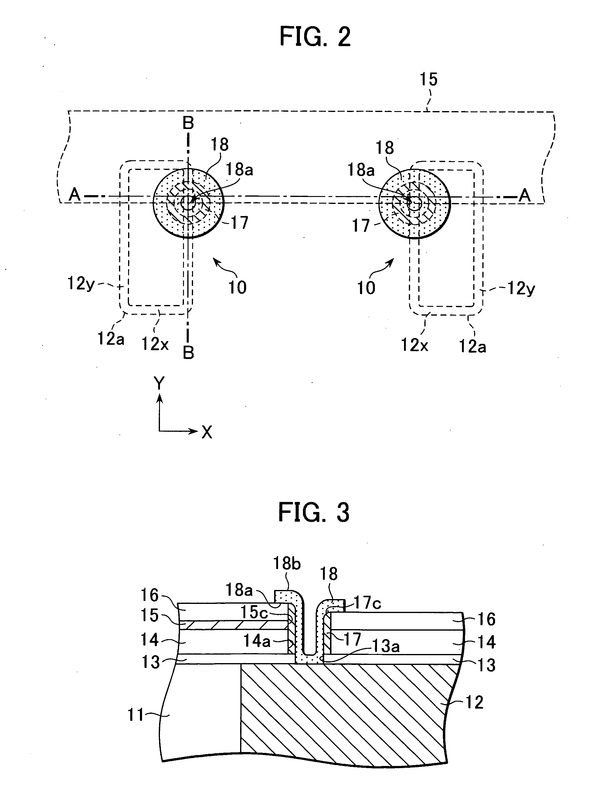
[0062]FIG. 1 is a cross-sectional view of the structure of a memory cell using the non-volatile memory element 10 according to the present invention. FIG. 2 is a plan view of the memory element 10. A cross-sectional view along the line A-A shown in FIG. 2 is shown in FIG. 1. FIG. 3 is a cross-sectional view along the line B-B shown in FIG. 2.

[0063] With reference to FIG. 1, the non-volatile memory element 10 according to this embodiment of the present invention includes an interlayer insulation layer 11, a bottom electrode 12 buried in the interlayer insulation layer 11, a first etching stopper 13, interlayer insulation layer 14, bit line 15 and second etching stopper 16 formed in that order on the bottom electrode 12, a top electrode 17 provided on the inside wall of a through-hole 14a, and a recording layer 18 in contact with the bottom electrode 12 and the top electrode 17.

[0064] A material such as silicon oxide or silicon nitride can be used for the interlayer insulation layers...

second embodiment

[0112] A non-volatile memory element 20 according to the present invention will now be described.

[0113]FIG. 15 is a cross-sectional view of the structure of a memory cell using the non-volatile memory element 20 of this embodiment.

[0114] As shown in FIG. 15, the memory element 20 of this embodiment differs from the memory element 10 of the first embodiment shown in FIG. 1 in that it has no second etching stopper 16, the bit line 15 is provided over the through-hole 14a, and the through-hole 14a is filled with. insulation material 21. Other parts are the same as those of the memory element 10 and are denoted using the same symbols, so further explanation thereof is omitted.

[0115] Since in this embodiment the bit line 15 is provided over the through-hole 14a, the bit line 15 and top electrode 17 are connected vertically. Between the bit line 15 and the recording layer 18 is the insulation material 21 that fills the through-hole 14a, so there is no direct contact between the bit line...


PUM


Abstract

A non-volatile memory element comprising a bottom electrode 12, a top electrode 17 provided on the bottom electrode 12, and a recording layer 18 containing phase change material connected between the bottom electrode 12 and the top electrode 17. In accordance with this invention, the top electrode 17 is in contact with a growth initiation surface 18a of the recording layer 17. This structure can be obtained by forming the top electrode 17 before the recording layer 18, resulting in a three-dimensional structure. This decreases heat dissipation to the bit line without increasing the thickness of the recording layer 18.

Description

TECHNICAL FIELD [0001] The present invention relates to an electrically rewritable non-volatile memory element and to a method of manufacturing the element. More specifically, the present invention relates to an electrically rewritable non-volatile memory element having a recording layer that includes phase change material, and to a method of manufacturing the element. BACKGROUND OF THE INVENTION [0002] Personal computers and servers and the like use a hierarchy of memory devices. There is lower-tier memory, which is inexpensive and provides high storage capacity, while memory higher up the hierarchy provides high-speed operation. The bottom tier generally consists of magnetic storage such as hard disks and magnetic tape. In addition to being non-volatile, magnetic storage is an inexpensive way of storing much larger quantities of information than solid-state devices such as semiconductor memory. However, semiconductor memory is much faster and can access stored data randomly, in co...

Claims


Application Information

Patent Timeline
Patent Type & Authority Applications(United States)
IPC IPC(8): G11C11/00
CPCG11C11/5678G11C13/0004G11C2213/52H01L45/06H01L45/1233H01L45/126H01L45/143H01L45/144H01L45/148H01L45/1675H01L45/122H10N70/821H10N70/231H10N70/8413H10N70/8825H10N70/826H10N70/884H10N70/8828H10N70/063
Inventor ASANO, ISAMULOWREY, TYLER A.
Owner MICRON TECH INC
Why Eureka
Try Eureka