Strain-compensated metastable compound base heterojunction bipolar transistor

a compound base, bipolar transistor technology, applied in the direction of basic electric elements, electrical apparatus, semiconductor devices, etc., can solve the problems of reducing device performance, limiting the amount of ge that can be added to the si lattice, and high cost of the gaas device, so as to achieve greater energy band offset, improve current densities, and increase the effect of ge fraction

Inactive Publication Date: 2007-05-10
ATMEL CORP
View PDF94 Cites 23 Cited by
  • Summary
  • Abstract
  • Description
  • Claims
  • Application Information

AI Technical Summary

Benefits of technology

[0014] The present invention is a method for pseudomorphic growth and integration of a strain-compensated metastable and/or unstable compound base, which may also be in-situ doped, into an electronic device, such as, for example, a SiGe NPN HBT, by substitutional and/or interstitial placement of strain-compensating atomic species. The method allows for control of defect density, and thus resultant con

Problems solved by technology

However, GaAs devices are relatively high in cost and cannot achieve the level of integration, such as, for example, of BiCMOS devices.
However, there is a limit to how much Ge can be added to the Si lattice before excess strain relaxation and gross crystalline defects occur.
If not controlled, a resultant poor crystal quality due to lattice imperfections will degrade device performance.
“Bridging” defects will also lead to excessive leakage current along with extremely low cu

Method used


Image

  • Strain-compensated metastable compound base heterojunction bipolar transistor
  • Strain-compensated metastable compound base heterojunction bipolar transistor
  • Strain-compensated metastable compound base heterojunction bipolar transistor

Examples


Embodiment Construction

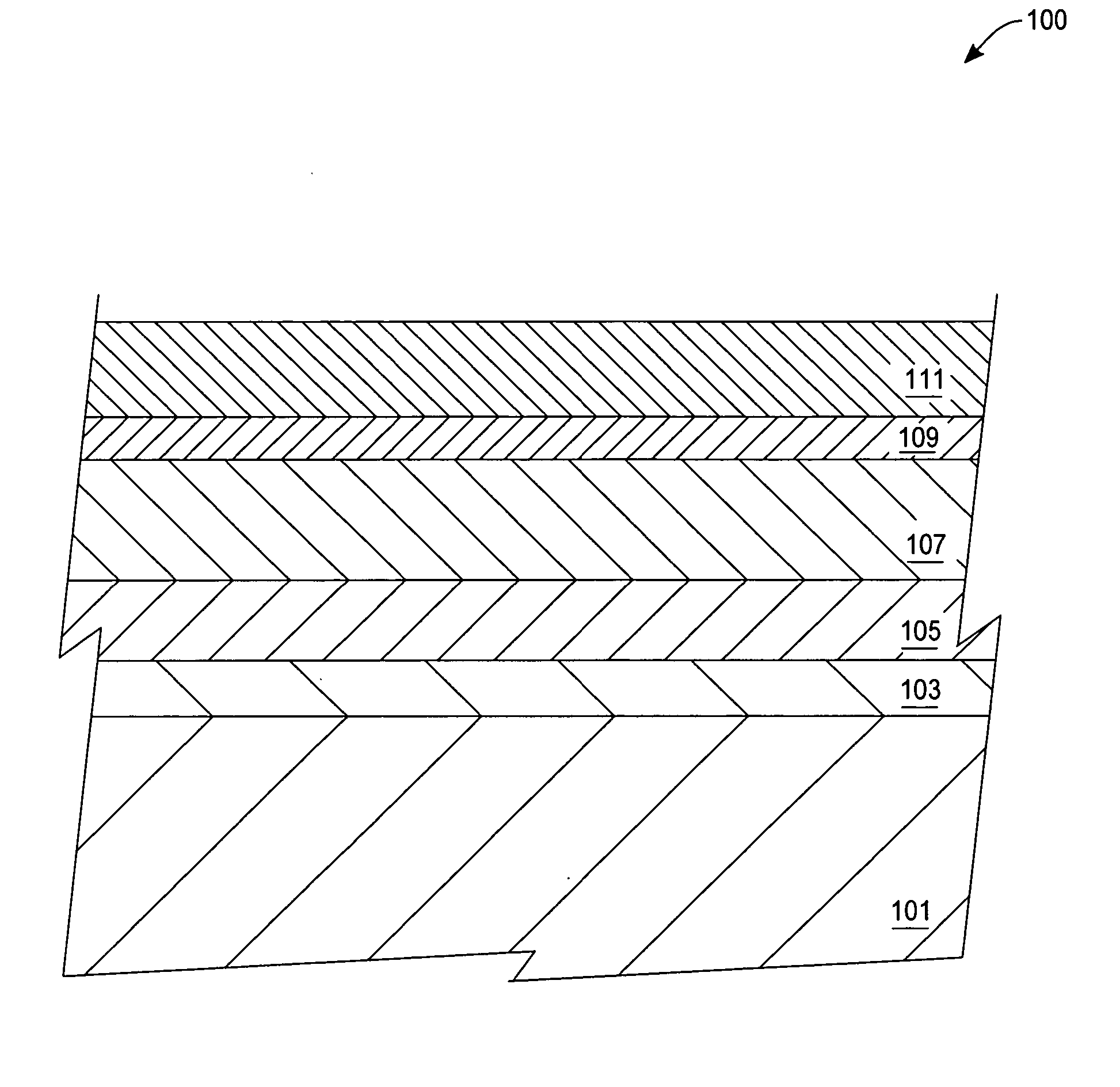
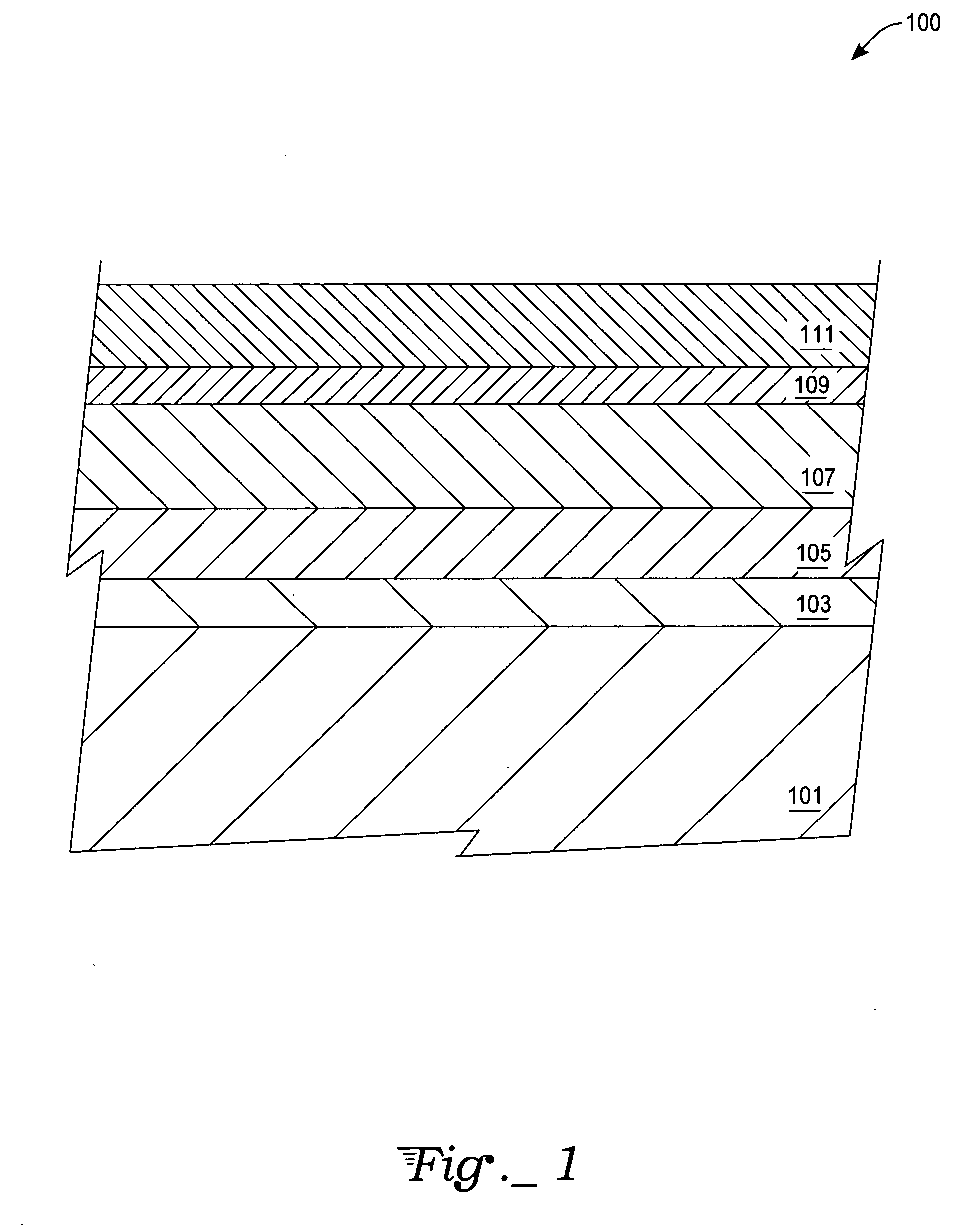
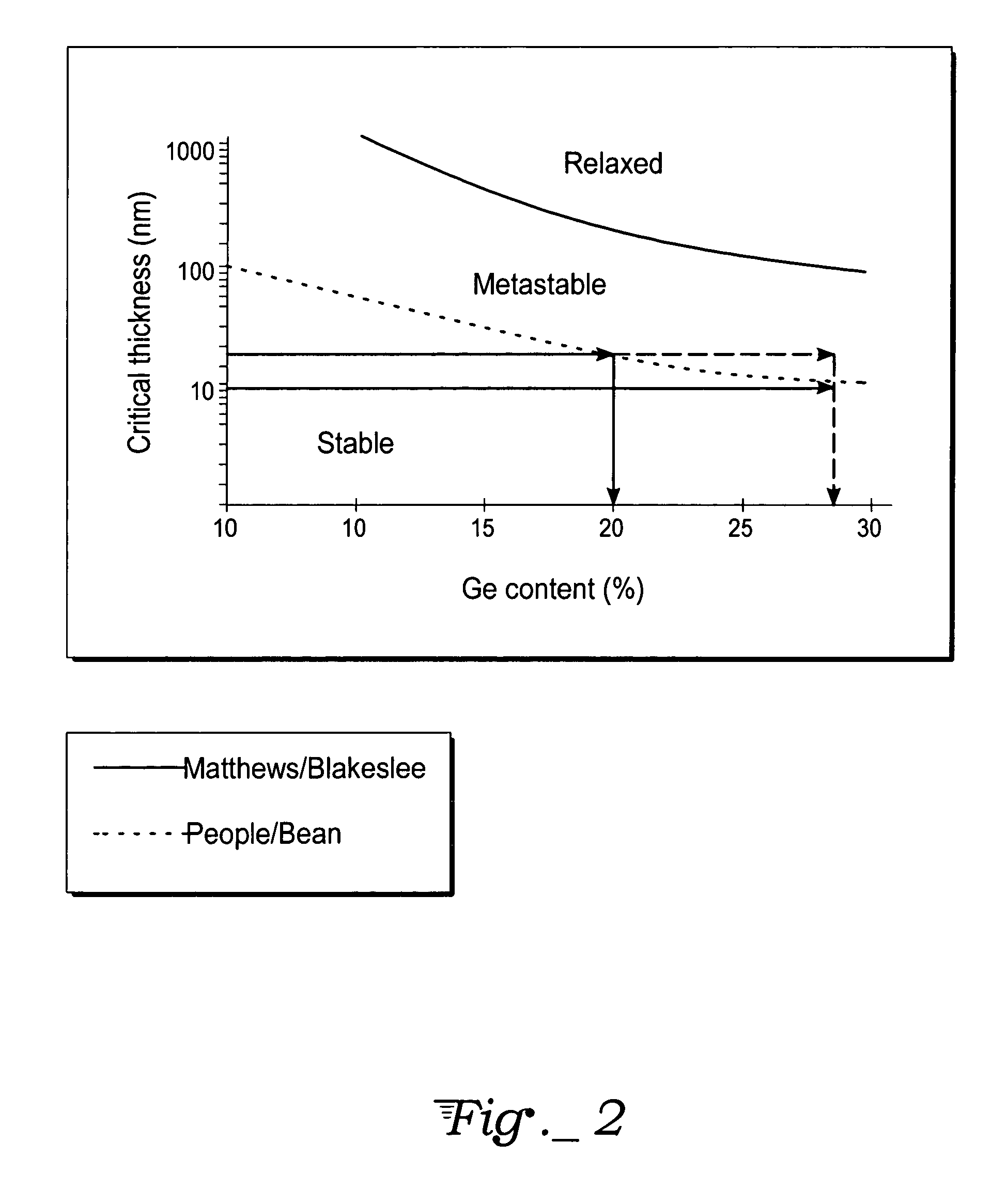
[0022] A strain-compensating atomic species is a species that, when added, alters the lattice parameter of a crystalline film from its intrinsic value. The intrinsic lattice parameter is the lattice parameter of the film or layer without the strain compensating species. For strain compensation of SiGe, one strain-compensating atomic species is carbon. One atomic percent of substitutional carbon will compensate eight percent to ten percent of Ge. Additionally, carbon can be substitutionally placed to approximately 2.5 percent in SiGe, or enough carbon to strain compensate 20 to 25 percent of Ge. Therefore, pseudomorphic strain-compensated metastable and / or unstable films with Ge levels of greater than 40 percent are possible (i.e., using four percent to five percent carbon) for electronic device use.

[0023] Even though one exemplary embodiment provides for strain reduction, a strain compensating atomic species with a larger lattice constant than either Si or Ge could be added to purp...


PUM


Abstract

A method for pseudomorphic growth and integration of an in-situ doped, strain-compensated metastable compound base into an electronic device, such as, for example, a SiGe NPN HBT, by substitutional placement of strain-compensating atomic species. The invention also applies to strained layers in other electronic devices such as strained SiGe, Si in MOS applications, vertical thin film transistors (VTFT), and a variety of other electronic device types. Devices formed from compound semiconductors other than SiGe, such as, for example, GaAs, InP, and AlGaAs are also amenable to beneficial processes described herein.

Description

TECHNICAL FIELD [0001] The invention generally relates to methods of fabrication of integrated circuits (ICs). More specifically, the invention is a method of fabricating and integrating a metastable silicon-germanium (SiGe) base region into a heterojunction bipolar transistor (HBT). BACKGROUND ART [0002] The SiGe HBT has significant advantages over a silicon (silicon) bipolar junction transistor (BJT) in gain, frequency response, noise parameters, and retains an ability to integrate with CMOS devices at relatively low cost. Cutoff frequencies (Ft) of SiGe HBT devices have been reported to exceed 300 GHz, which is favorable as compared to GaAs devices. However, GaAs devices are relatively high in cost and cannot achieve the level of integration, such as, for example, of BiCMOS devices. The silicon compatible SiGe HBT provides a low cost, high speed, low power solution that is quickly replacing other compound semiconductor devices. [0003] Advantages of SiGe are realized by a bandgap ...

Claims


Application Information

Patent Timeline
IPC IPC(8): H01L21/20
CPCH01L29/66242H01L29/7842H01L21/20H01L29/737
Inventor ENICKS, DARWIN G.CHAFFEE, JOHN T.CARVER, DARNIAN A.
Owner ATMEL CORP
Why Eureka
Try Eureka