Gate structure and fabricating method thereof

Active Publication Date: 2007-05-10
PROMOS TECH INC
View PDF4 Cites 38 Cited by
  • Summary
  • Abstract
  • Description
  • Claims
  • Application Information

AI Technical Summary

Benefits of technology

[0012] Accordingly, at least one objective of the present invent

Problems solved by technology

Ultimately, the performance o

Method used


Image

  • Gate structure and fabricating method thereof
  • Gate structure and fabricating method thereof
  • Gate structure and fabricating method thereof

Examples


Example

[0036] Reference will now be made in detail to the present preferred embodiments of the invention, examples of which are illustrated in the accompanying drawings. Wherever possible, the same reference numbers are used in the drawings and the description to refer to the same or like parts.

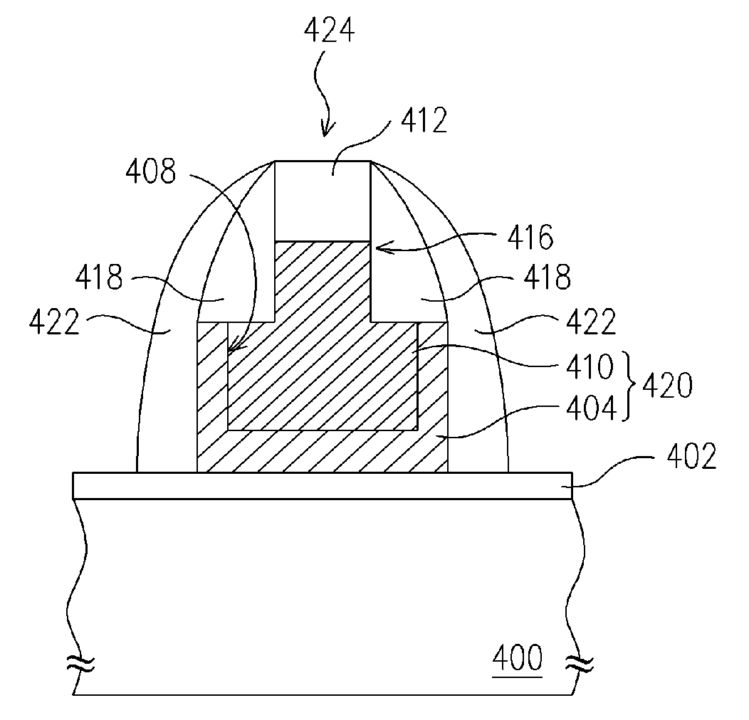
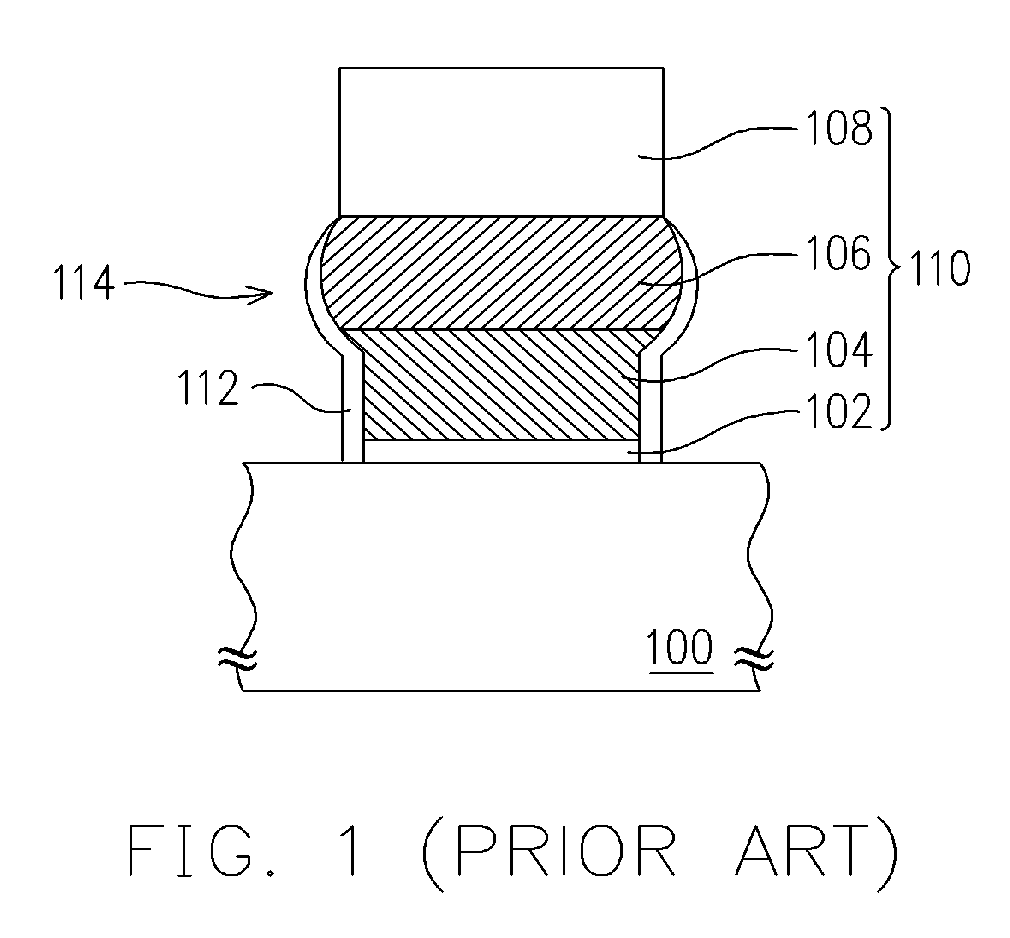
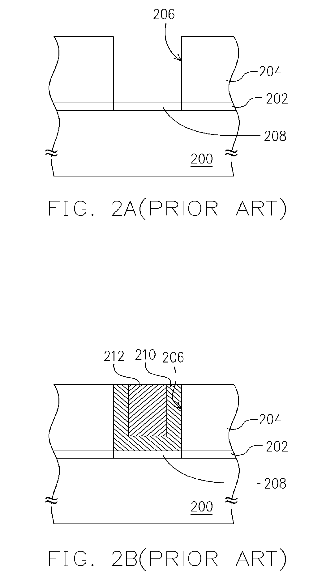
[0037]FIG. 3 is a schematic cross-sectional view of a gate structure according to one embodiment of the present invention. As shown in FIG. 3, the gate structure 320 includes a substrate 300, a gate dielectric layer 302, a first conductive layer 304, a second conductive layer 308, a cap layer 314 and a pair of spacers 316.

[0038] The gate dielectric layer 302 is disposed on the substrate 300. The gate dielectric layer 302 is fabricated using silicon oxide or any other suitable material, for example.

[0039] The first conductive layer 304 is disposed over the gate dielectric layer 302. Furthermore, the first conductive layer 304 has an opening 306. The first conductive layer 304 is fabricated using d...


PUM

PropertyMeasurementUnit
Electrical conductoraaaaaaaaaa
Widthaaaaaaaaaa

Abstract

A gate structure comprising a substrate, a gate dielectric layer, a first conductive layer, a second conductive layer, a cap layer and a first insulating spacer is provided. The gate dielectric layer is disposed on the substrate. The first conductive layer is disposed on the gate dielectric layer and has an opening. Part of the second conductive layer is disposed in the opening. The second conductive layer has an extrusion that protrudes above the opening of the first conductive layer. The extrusion has a cross-sectional width less than the width of the second conductive layer inside the opening. The cap layer is disposed on the extrusion. The first insulating spacer is disposed on part of the first conductive layer and covers the sidewalls of the extrusion. The inclusion of the extrusion in the second conductive layer decreases the resistance of the gate structure and promotes the efficiency of the device.

Description

CROSS-REFERENCE TO RELATED APPLICATION [0001] This application claims the priority benefit of Taiwan application serial no. 941 39231, filed on Nov. 9, 2005. All disclosure of the Taiwan application is incorporated herein by reference. BACKGROUND OF THE INVENTION [0002] 1. Field of the Invention [0003] The present invention relates to a semiconductor device structure. More particularly, the present invention relates to a gate structure. [0004] 2. Description of the Related Art [0005] Because of the high level of integration of deep sub-micron integrated circuits, many device features including line width, contact area and junction depth have been substantially reduced. To increase the performance of the devices despite of such reduction, lowering the resistance and reducing signal delay due to resistance and capacitance (RC-delay) has become immensely important. Thus, in the fabrication of semiconductor devices, a refractory metal silicide layer is frequently formed on polysilicon g...

Claims


Application Information

Patent Timeline
IPC IPC(8): H05K3/00B05D1/32B05D1/36
CPCH01L21/28061H01L21/28114H01L29/42376H01L29/6656H01L29/66583
Inventor LAI, SU-CHEN
Owner PROMOS TECH INC
Why Eureka
Try Eureka