Ion implantation ion source, system and method

a technology of ion implantation and ion source, which is applied in the direction of ion beam tubes, electrical equipment, discharge tubes, etc., can solve the problems of preventing effective implanting of dopant species, inefficient ion implantation implanters, and low energy transport efficiency of ion implanters, so as to maximize the electron flow through the ionization chamber, reduce the effect of ionization chamber ionization and ionization chamber size and size, and reduce the effect of i

Inactive Publication Date: 2007-05-17
SEMEQUIP
View PDF37 Cites 26 Cited by
  • Summary
  • Abstract
  • Description
  • Claims
  • Application Information

AI Technical Summary

Benefits of technology

[0128] In a high current design an acceleration-deceleration system aligned with the direction of transit through the ionization chamber is advantageous in a number of respects, especially when employing an accel-decel system for maximizing the electron flow through the ionization chamber.
[0129] The electron beam, however produced, has a significant cross-sectional area, i.e. it is a broad generally collimated beam as it transits the ionization chamber, to the beam dump with which it is aligned. In preferred embodiments, the electron beam within the ionization chamber has a generally rectangular cross section, e.g. in one embodiment approximately 13 mm×6 mm as injected into the ionization chamber, to match with a relatively wide extraction aperture of a high current machine, or the rectangular cross section is e.g. of a square cross-section profile for use with a narrower ion extraction aperture. In the case of direct injection, the shape of the injected...

Problems solved by technology

A very significant problem which currently exists in the ion implantation of semiconductors is the limitation of production-worthy ion implantation implanters that prevents effective implanting of dopant species at low (e.g., sub-keV) energies at commercially desired rates.
Ion implanters are relatively inefficient at transporting low-energy ion beams due to space charge within the ion beam, the lower the energy, the greater the problem.
When the beam profile exceeds the profile for which the implanter's transport optics have been designed, beam loss through vignetting occurs.
For example, at 500 eV transport energy, many ion implanters currently in use cannot transport enough boron beam current to be commercially efficient in manufacturing; i.e., the wafer throughput is too low because of low implantation dose rate.
Since this magnetic field also ...

Method used


Image

  • Ion implantation ion source, system and method
  • Ion implantation ion source, system and method
  • Ion implantation ion source, system and method

Examples


Embodiment Construction

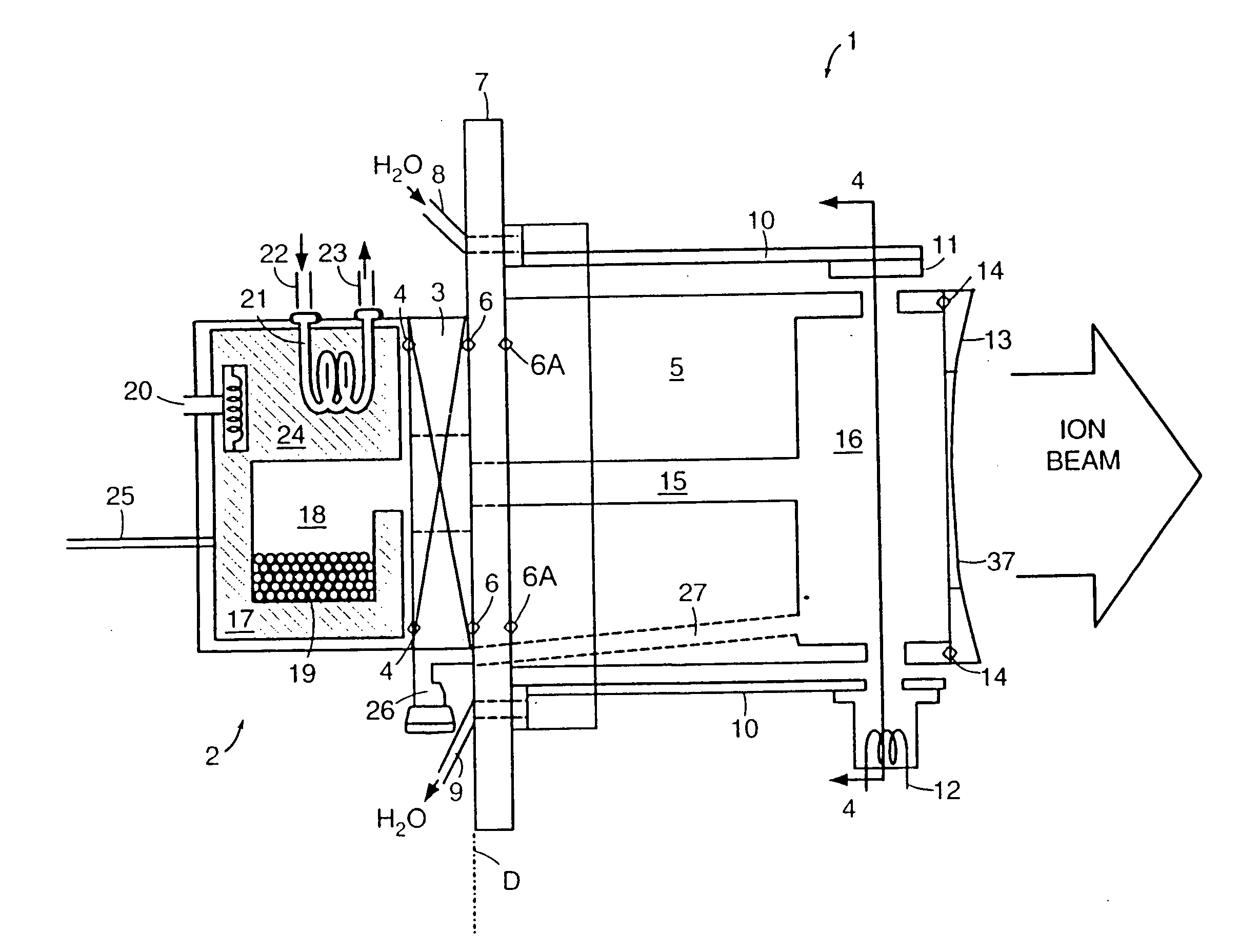
[0172]FIG. 3 shows in schematic an embodiment of ion source 1. The vaporizer 2 is attached to the vaporizer valve 3 through an annular thermally conductive gasket 4. The vaporizer valve 3 is likewise attached to the mounting flange 7, and the mounting flange 7 is attached to ionization chamber body 5 by further annular thermally conductive gaskets 6 and 6A. This ensures good thermal conduction between the vaporizer, vaporizer valve, and ionization chamber body 5 through intimate contact via thermally conductive elements. The mounting flange 7 attached to the ionization chamber 5, e.g., allows mounting of the ion source 1 to the vacuum housing of an ion implanter, (see FIG. 8) and contains electrical feedthroughs (not shown) to power the ion source, and water-cooling feedthroughs 8, 9 for cooling. In this preferred embodiment, water feedthroughs 8, 9 circulate water through the cooled mounting frame 10 to cool the mounting frame 10 which in turn cools the attached components, the ele...


PUM

PropertyMeasurementUnit
Lengthaaaaaaaaaa
Lengthaaaaaaaaaa
Lengthaaaaaaaaaa

Abstract

Various aspects of the invention provide improved approaches and methods for efficiently: Vaporizing decaborane and other heat-sensitive materials via a novel vaporizer and vapor delivery system; Delivering a controlled, low-pressure drop flow of vapors, e.g. decaborane, into the ion source;
Ionizing the decaborane into a large fraction of B10Hx+; Preventing thermal dissociation of decaborane;
Limiting charge-exchange and low energy electron-induced fragmentation of B10Hx+; Operating the ion source without an arc plasma, which can improve the emittance properties and the purity of the beam; Operating the ion source without use of a strong applied magnetic field, which can improve the emittance properties of the beam; Using, a novel approach to produce electron impact ionizations without the use of an arc discharge, by incorporation of an externally generated, broad directional electron beam which is aligned to pass through the ionization chamber to a thermally isolated beam dump;. Providing production-worthy dosage rates of boron dopant at the wafer; Providing a hardware design that enables use also with other dopants, especially using novel hydride, dimer-containing, and indium- or antimony-containing temperature-sensitive starting materials, to further enhance the economics of use and production worthiness of the novel source design and in many cases, reducing the presence of contaminants; Matching the ion optics requirements of the installed base of ion implanters in the field; Eliminating the ion source as a source of transition metals contamination, by using an external and preferably remote cathode and providing an ionization chamber and extraction aperture fabricated of non-contaminating material, e.g. graphite, silicon carbide or aluminum; Enabling retrofit of the new ion source into the ion source design space of existing Bernas source-based ion implanters and the like or otherwise enabling compatibility with other ion source designs; Using a control system in retrofit installations that enables retention of the installed operator interface and control techniques with which operators are already familiar; Enabling convenient handling and replenishment of the solid within the vaporizer without substantial down-time of the implanter; Providing internal adjustment and control techniques that enable, with a single design, matching the dimensions and intensity of the zone in which ionization occurs to the beam line of the implanter and the requirement of the process at hand; Providing novel approaches, starting materials and conditions of operation that enable the making of future generations of semiconductor devices and especially CMOS source/drains and extensions, and doping of silicon gates.

Description

CROSS-REFERENCE TO RELATED APPLICATIONS [0001] This application claims priority of and benefit of U.S. Provisional Patent Application No. 60 / 170,473 filed on Dec. 13, 1999, U.S. Provisional Patent Application No. 60 / 250,080 filed on Nov. 30, 2000 and PCT Patent Application No. PCT / US00 / 33786 filed on Dec. 13, 2000.BACKGROUND OF THE INVENTION [0002] 1. Field of Invention [0003] The invention provides production-worthy ion sources and methods capable of using new source materials, in particular, heat-sensitive materials such as decaborane (B10H14), and hydrides and dimer-containing compounds novel to the ion implantation process, to achieve new ranges of performance in the commercial ion implantation of semiconductor wafers. The invention enables shallower, smaller and higher densities of semiconductor devices to be manufactured, particularly in Complementary Metal-Oxide Semiconductor (CMOS) manufacturing. In addition to enabling greatly enhanced operation of new ion implanter equipme...

Claims


Application Information

Patent Timeline
IPC IPC(8): C23F1/00
CPCH01J27/205H01J37/08H01J2237/082H01J2237/0835H01J2237/31701
Inventor HORSKY, THOMAS NEILWILLIAMS, JOHN NOEL
Owner SEMEQUIP
Why Eureka
Try Eureka