Novel method for four direction low capacitance ESD protection

a technology of esd protection and four-direction manufacturing process, which is applied in the direction of semiconductor devices, semiconductor/solid-state device details, diodes, etc., can solve the problems of severe esd damage of field effect transistors (fet) devices, and achieve low capacitance, improve esd protection, and reduce the capacitance of protective devices

Inactive Publication Date: 2007-05-17
TAIWAN SEMICON MFG CO LTD
View PDF27 Cites 5 Cited by
  • Summary
  • Abstract
  • Description
  • Claims
  • Application Information

AI Technical Summary

Benefits of technology

[0017] Accordingly, it is the primary objective of the invention to provide an effective and manufacturable method and structure for reducing the capacitance of the protective device providing resistance to the potential damage caused by the phenomenon known as electrostatic discharge (ESD) by utilizing a low capacitance ESD protection device connected to an input pad of an integrated circuit device.
[0018] It is a further objective of the invention to improve ESD protection for high frequency applications by providing a low input capacitance structure that will have minimum impact on device performance while maintaining reasonable ESD protection levels.
[0019] A still additional objective of the invention is to provide the ESD protection with reduced capacitance without changing the characteristics of the internal circuits being protected and by using a process compatible with the process of integrated MOS device manufacturing.
[0020] The above objectives are achieved in accordance with the methods of the invention that describes a structure and a manufacturing process for semiconductor ESD protection devices with reduced input capacitance. One embodiment of the invention utilizes a NMOS FET structure with associated junction diode and parasitic NPN bipolar transistor for ESD protection for both positive and negative ESD voltages occurring on the active circuit input pad. There is a heavily doped P+ guard ring that protects the NMOS device from exhibiting latchup characteristics. The guard ring also enhances the junction diode characteristics improving ESD protection for negative ESD voltages on the input pad. A heavily doped N+ guard ring surrounding the NMOS device including the P+ guard ring enhances the Vcc to Vss ESD protection diode characteristics, and eliminates the need for an additional device, often referred to as ESD2, to protect against this mode of ESD occurrence, which would normally be attached from the input pad to Vcc. This design structure eliminates the capacitance associated with the prior art devices that have a second ESD protection device from the input pad to Vcc.

Problems solved by technology

Because of high input impedance and thin oxide gate structures, the problem of electrostatic discharge damage (ESD) with field effect transistor (FET) devices can be severe.

Method used


Image

  • Novel method for four direction low capacitance ESD protection
  • Novel method for four direction low capacitance ESD protection
  • Novel method for four direction low capacitance ESD protection

Examples


Embodiment Construction

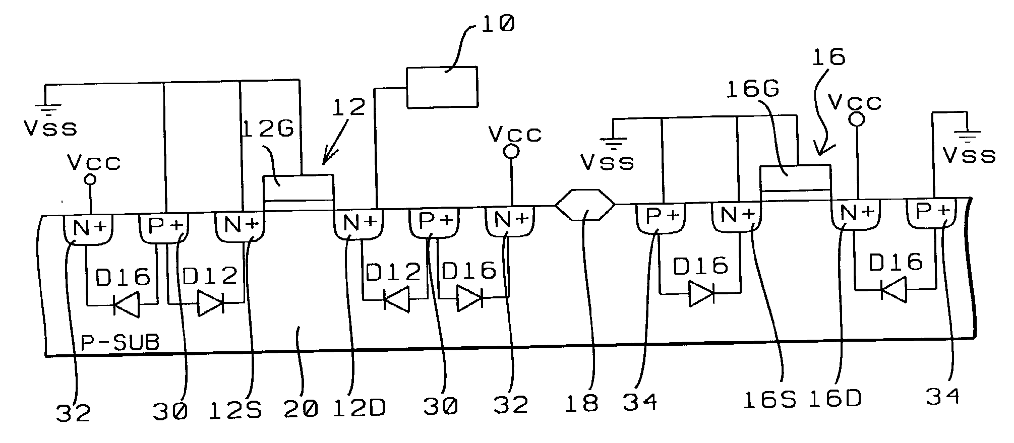
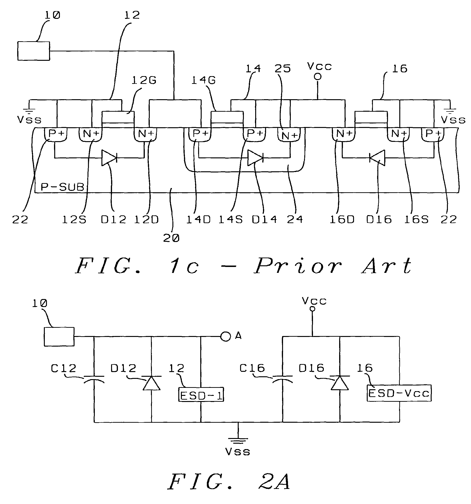
[0030]FIG. 2A shows a simplified representation of the principle advantage of the invention. As shown in FIG. 2A, the input pad 10 is protected from ESD incidents by the protection devices ESD-1 element 12. The invention embodiment details are sufficient to protect the input circuit from both positive and negative ESD voltage events. In addition, the embodiment of the invention also protects against positive and negative ESD voltages that may occur on the Vcc and or on the Vss power bus.

[0031]FIG. 2B shows typical device schematic devices for a NMOS device 12 used for the protective devices ESD-1. The NMOS 12 drain 12D is connected to the input pad 10, and the source 12S and gate 12G are connected to a second voltage source Vss, typically ground. Shown electrically in parallel with ESD-1 NMOS device 12 are the parasitic elements diode D12 and capacitor C12 connected between the input pad 10 and the second voltage source, Vss. Also shown in FIG. 2B is the bipolar NPN parasitic trans...


PUM


Abstract

The invention describes a structure and a process for providing ESD semiconductor protection with reduced input capacitance. The structure consists of heavily doped P+ guard rings surrounding the I / O ESD protection device and the Vcc to Bss protection device. In addition, there is a heavily doped N+ guard ring surrounding the I / O protection device its P+ guard ring. The guard rings enhance structure diode elements providing enhanced ESD energy discharge path capability enabling the elimination of a specific conventional Vss to I / O pad ESD protection device. This reduces the capacitance seen by the I / O circuit while still providing adequate ESD protection for the active circuit devices.

Description

CROSS REFERENCE TO RELATED APPLICATIONS [0001] This application is a division of pending U.S. patent application Ser. No. 10 / 207,545, filed Jul. 29, 2002 and entitled “A NOVEL METHOD FOR FOUR DIRECTION LOW CAPACITANCE ESD PROTECTION”.BACKGROUND OF THE INVENTION [0002] 1. Field of the Invention [0003] The present invention relates generally to the structure and manufacturing process of a FET semiconductor device for ESD protection of electronic circuit devices and more particularly to a structure with a guard ring for low capacitance input ESD protection. [0004] 2. Description of Prior Art [0005] Because of high input impedance and thin oxide gate structures, the problem of electrostatic discharge damage (ESD) with field effect transistor (FET) devices can be severe. Therefore the input / output (I / O) circuit locations or pads usually have a protective device connected between the I / O pad and the internal circuits which allows the ESD current to be shunted to an alternative voltage sou...

Claims


Application Information

Patent Timeline
Patent Type & Authority Applications(United States)
IPC IPC(8): H01L23/62
CPCH01L27/0255
Inventor LEE, JIAN-HSINGCHEN, SHUI HUN YI
Owner TAIWAN SEMICON MFG CO LTD
Why Eureka
Try Eureka