

OLEDS with improved efficiency
a technology of oleds and efficiency, applied in the direction of discharge tube luminescnet screens, natural mineral layered products, transportation and packaging, etc., can solve the problems of insufficient el efficiency, potential limit factor of el efficiency of oled devices, and inability to explain the advantages of such a structure, etc., to achieve the effect of improving luminance yield
- Summary
- Abstract
- Description
- Claims
- Application Information
AI Technical Summary
Benefits of technology
Problems solved by technology
Method used
Image

Examples
examples t1-t8
Test devices
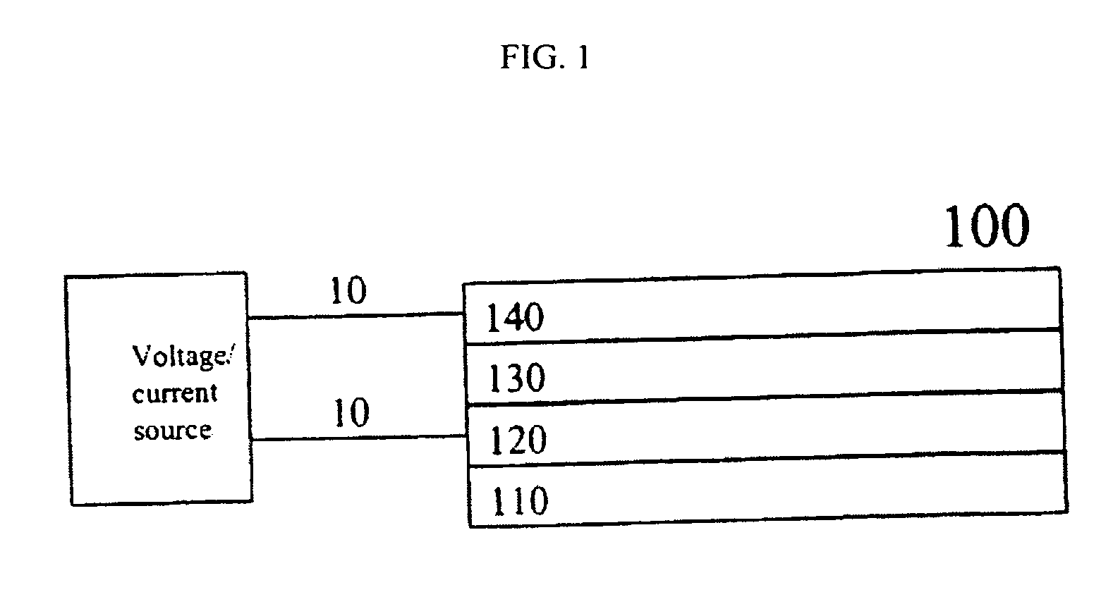
[0462] OLED devices T1-T8 (Table 1) were prepared as follows. A glass substrate coated with ˜250 Å transparent indium-tin-oxide (ITO) conductive layer was cleaned and dried using a commercial glass scrubber tool. The ITO surface was subsequently treated with oxygen plasma to condition the surface as an anode. Over the ITO was deposited a ˜10 Å thick hole-injecting layer of fluorocarbon (CFx) by plasma-assisted deposition of CHF3. The following layers were deposited in the following sequence by sublimation from heated crucible boats in a conventional vacuum deposition chamber under a vacuum of approximately 10−6 Torr (Table 1): [0463] (1) the HTL, 750 Å thick, composed of NPB; [0464] (2) the light-emitting layer, 375 Å thick, composed of AlQ; [0465] (3) the ETL, 375 Å thick, composed of either AlQ (reference device Ti), AlQ doped with 3.7% Li, or a test ETL material, which is either undoped or doped with 3.7% Li; [0466] (4) the cathode, 2,100 Å thick, including an alloy ...
##ventive examples 1-32
Comparative and Inventive Examples 1-32
Blue OLEDs
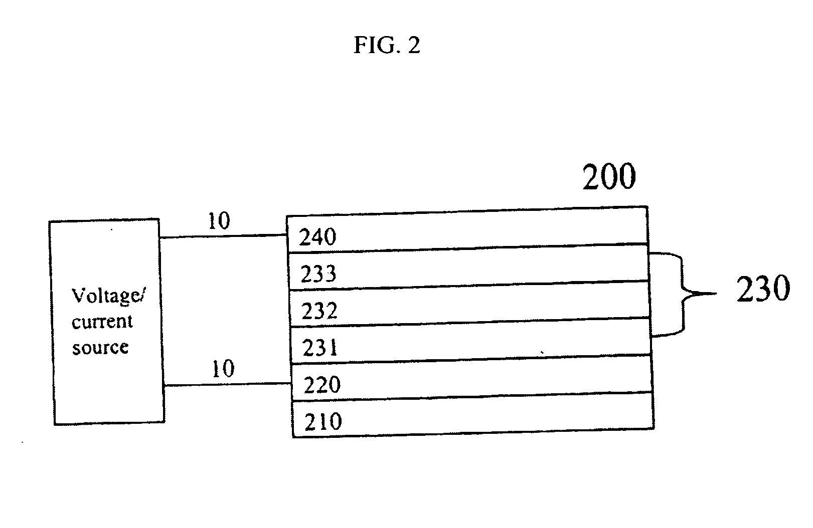
[0471] OLED devices 1-16 were prepared similarly to the test devices T1-T8, except for layers 1, 2, and 3, and used the same anode and the same cathode. The following layers were deposited in the following sequence (Table 2): [0472] (1) where present, the first HTL composed of either 450 Å mTDATA or 550 Å mTDATA doped with 3% of F4TCNQ; [0473] (2) the second HTL, either 750, 300, or 200 Å thick, composed of NPB; [0474] (3) the light-emitting layer, 400 Å thick, including
[0475] (i) TBADN as the host,
[0476] (ii) either 0.8% of Blue-2 or 1% of TBP as the dopant, and
[0477] (iii) where present, NPB as the hole-trapping material in certain % (indicated in Table 2; the range indicates that the performance of devices having NPB % in this range was found similar); [0478] (4) where present, the first ETL, either 200 or 50 Å thick, composed of either AlQ or BPhen; [0479] (5) where present, the second ETL, either 200 or 150 Å thick, composed ...
##ventive examples 33-43
Comparative and Inventive Examples 33-43
Blue-green OLEDs
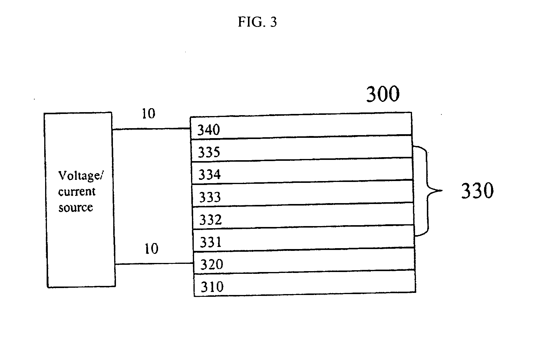
[0490] OLED devices 33-43 were prepared similarly to the devices 1-15, except: [0491] (i) in place of Blue-2 or TBP, Blue-green-2 was used as the dopant; [0492] (ii) either TBADN, BPNA, 2,2′(DPA)2, or ADN were used as the LEL host; and [0493] (iii) only AlQ or AlQ+3.7% Li were used as ETL materials.
[0494] As can be seen from Table 2, the EL efficiencies (cd / A and W / A) for the simpler comparative devices 33-37, having an ordinary ETL, are relatively low, 0.095-0.105 W / A.
[0495] As can be further seen from Table 2, the EL efficiency for the comparative device 38, having an improved ETL composition, is higher, 0.120 W / A. Addition of a hole-trapping material to the LEL, as in device 39, leads to a further increase to 0.134 W / A.
[0496] As can be further seen from Table 2, the EL efficiencies for the inventive devices 40 and 41, having a host, a hole-trapping material, and a dopant in their LEL's, two HTL's as specified in the curr...
PUM
| Property | Measurement | Unit |
|---|---|---|
| Percent by volume | aaaaa | aaaaa |
| Percent by volume | aaaaa | aaaaa |
| Percent by volume | aaaaa | aaaaa |
Abstract
Description
Claims
Application Information