Paraelectric thin film structure for high frequency tunable device and high frequency tunable device with the same

a thin film structure and high-frequency tunable technology, applied in the direction of thin/thick film capacitors, capacitors with voltage varied dielectrics, fixed capacitors, etc., can solve the problems of high driving voltage of ferroelectric films, high frequency dielectric loss, frequency/phase tuning rate, etc., to improve high-frequency response characteristics, reduce the effect of dielectric loss and large dielectric constant tuning ra

Inactive Publication Date: 2007-06-14
ELECTRONICS & TELECOMM RES INST
View PDF11 Cites 15 Cited by
  • Summary
  • Abstract
  • Description
  • Claims
  • Application Information

AI Technical Summary

Benefits of technology

[0009] The present invention provides a paraelectric thin film structure having a large dielectric constant tuning rate and low dielectric loss for a high frequency tunable device.
[0010] The present invention also provides a paraelectric thin film structure having large dielectric constant tuning rate, low dielectric loss, and low temperature dependency in the dielectric constant, for a high frequency tunable device.
[0011] The present invention further provides a high frequency tunable device having improved microwave characteristics and high-speed, low-power-consuming, and low-cost characteristics by using a paraelectric thin film structure having a large dielectric constant tuning rate and low dielectric loss.
[0017] According to the present invention, the paraelectric thin film structure for the high frequency tunable device has a small lattice constant mismatch between the paraelectric film and the oxide single crystal substrate so that the paraelectric thin film structure can have a large dielectric constant tuning rate and low dielectric loss with respect to an external voltage input. Further, the high frequency tunable device can have improved high-frequency response characteristics by employing the paraelectric thin film structure, so that the high frequency tunable device can be usefully used in communication and sensor systems for high-speed, high-rate, next-generation broadband broadcastings, communications, and internet-based mobile wireless multimedia services.

Problems solved by technology

In developing such high frequency tunable devices with the ferroelectric films, high frequency dielectric loss, frequency / phase tuning rate, and high driving voltage of the ferroelectric film are main problems.
The ferroelectric hysteresis characteristic is a cause of error signals of the high frequency tunable device, thereby making it difficult to make the high frequency device.
However, obtaining a BST paraelectric film having characteristics comparable with the dielectric characteristics of a BST single crystal is limited.
Particularly, due to large lattice constant mismatch between the oxide single crystal substrate and the BST paraelectric film grown on the oxide single crystal substrate, epitaxial thin layer growth is not easy.
This causes a large strain / stress in the paraelectric film, thereby decreasing the dielectric constant tuning rate and increasing the dielectric loss.
Thus, high-frequency signal loss increases in the high frequency tunable device having the BST paraelectric film, such that it is difficult to attain devices having superior characteristics.

Method used


Image

  • Paraelectric thin film structure for high frequency tunable device and high frequency tunable device with the same
  • Paraelectric thin film structure for high frequency tunable device and high frequency tunable device with the same
  • Paraelectric thin film structure for high frequency tunable device and high frequency tunable device with the same

Examples


Embodiment Construction

[0035] The present invention will now be described more fully with reference to the accompanying drawings, in which exemplary embodiments of the invention are shown.

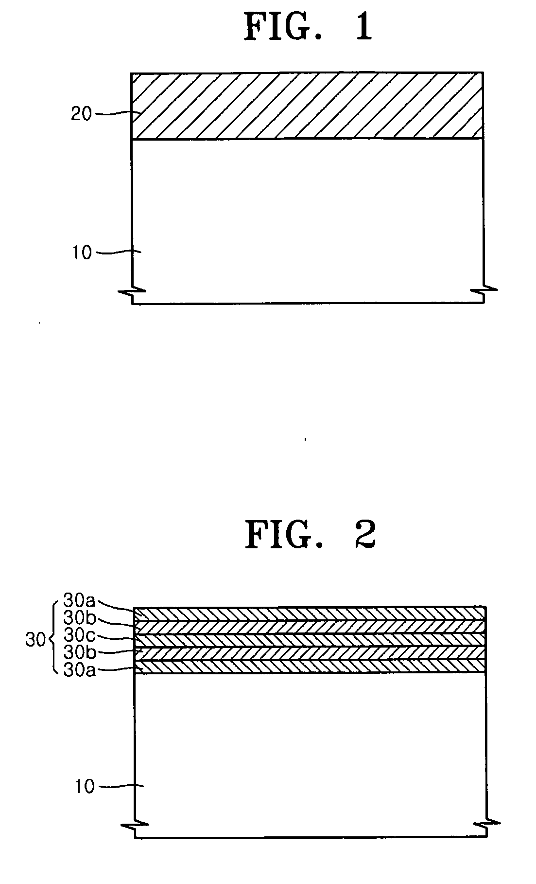
[0036]FIG. 1 is a sectional view of a paraelectric thin film structure including a paraelectric film formed on an oxide single crystal substrate for a high frequency tunable device according to the present invention, and FIG. 2 is a sectional view of a compositionally graded paraelectric thin film structure formed on an oxide single crystal substrate and including a plurality of paraelectric films for a high frequency tunable device according to the present invention.

[0037] Referring to FIG. 1, a paraelectric thin film structure for a high frequency tunable device of the present invention includes a perovskite ABO3 type paraelectric film 20 formed on an oxide single crystal substrate 10 to a predetermined thickness. The oxide single crystal substrate 10 includes MgO, LaAl2O3, or Al2O3 single crystal. The paraelectric f...


PUM

PropertyMeasurementUnit
thicknessaaaaaaaaaa
thicknessaaaaaaaaaa
thicknessaaaaaaaaaa

Abstract

Provided are a paraelectric thin film structure and a high frequency tunable device with the paraelectric thin film structure. The paraelectric thin film structure has a large dielectric constant tuning rate and a low dielectric loss at a high frequency. The paraelectric thin film structure includes a perovskite ABO3 type paraelectric film formed on an oxide single crystal substrate. The paraelectric film is formed of a material selected from Ba(Zrx,Ti1-x)O3, Ba(Hfy,Ti1-y)O3, or Ba(Snz,Ti1-z)O3. Instead of the paraelectric film, the paraelectric thin film structure may include a compositionally graded paraelectric film having at least two paraelectric films formed of the selected material by varying the composition ratio x, y, or z. A high-frequency / phase tunable device employing the paraelectric thin film structure can have improved microwave characteristics and high-speed, low-power-consuming, low-cost characteristics.

Description

CROSS-REFERENCE TO RELATED PATENT APPLICATION [0001] This application claims the benefit of Korean Patent Application Nos. 10-2005-0120174, filed on Dec. 8, 2005 and 10-2006-0007915, filed on Jan. 25, 2006, in the Korean Intellectual Property Office, the disclosures of which are incorporated herein in their entirety by reference. BACKGROUND OF THE INVENTION [0002] 1. Field of the Invention [0003] The present invention relates to a paraelectric thin film with a perovskite ABO3 structure and a high frequency tunable device using the paraelectric thin film. [0004] 2. Description of the Related Art [0005] Recently, various new services are realized, such as high-speed, high-rate, next-generation broadband broadcastings, communications, internet-based mobile wireless multimedia systems, ubiquitous communications, and sensor systems. Accordingly, development of high-speed, low-power-consuming, low-cost core materials / parts is important for wireless mobile / satellite communication and senso...

Claims


Application Information

Patent Timeline
Patent Type & Authority Applications(United States)
IPC IPC(8): H01L29/93H01L21/20
CPCH01G4/1227H01G4/33H01G7/06H01L21/31691H01L28/56H01L21/02197
Inventor LEE, SU JAERYU, HAN CHEOLMOON, SEUNG EONKIM, YOUNG TAEKWAK, MIN HWANKANG, KWANG YONG
Owner ELECTRONICS & TELECOMM RES INST
Why Eureka
Try Eureka