

Laser irradiation apparatus, laser irradiation method, and manufacturing method of semiconductor device
a laser irradiation and laser technology, applied in the direction of laser beam welding apparatus, manufacturing tools, welding/soldering/cutting articles, etc., can solve the problem of limited layout, achieve easy projecting of images, reduce the influence of optical axis displacement in the deflector, and achieve laser processing
- Summary
- Abstract
- Description
- Claims
- Application Information
AI Technical Summary
Benefits of technology
Problems solved by technology
Method used
Image

Examples
embodiment 1
[0067] Embodiment 1 will describe an example of conducting laser irradiation to a semiconductor film by synthesizing laser beams which have been emitted from a plurality of laser oscillators, in order to increase efficiency of laser irradiation.
[0068] Each of laser oscillators 401 and 402 of FIG. 8 is a mode-locked pulsed laser oscillator having an output power of 20 W, a repetition rate of 80 MHz, a pulse width of 20 to 30 psec, a wavelength of 532 nm, a beam diameter of 1 mm, and TEM00 mode (single transverse mode). The mode-locked pulsed laser oscillator has the repetition rate which is extremely higher than a repetition rate of several tens to several hundreds Hz of a conventional pulsed laser oscillator. It is said that it takes several tens to several hundreds nsec to completely solidify a semiconductor film after irradiating the semiconductor film with a pulsed laser beam. With the pulsed laser oscillator having a repetition rate of 10 MHz or more, the semiconductor film can...
embodiment 2
[0076] Embodiment 2 will describe an example of conducting laser irradiation by deflecting laser beams which have been emitted from a plurality of laser oscillators by deflectors and synthesizing a plurality of beam spots on an irradiation surface.
[0077] Each of laser oscillators 501 and 502 of FIG. 9 is a mode-locked pulsed laser oscillator having an output power of 10 W, a repetition rate of 80 MHz, a pulse width of 20 to 30 psec, a wavelength of 532 nm, a beam diameter of 1 mm, and TEM00 mode (single transverse mode). The mode-locked pulsed laser oscillator has the repetition rate which is extremely higher than a repetition rate of several tens to several hundreds Hz of a conventional pulsed laser oscillator. It is said that it takes several tens to several hundreds nsec to completely solidify a semiconductor film after irradiating the semiconductor film with a pulsed laser beam. With the pulsed laser oscillator having a repetition rate of 10 MHz or more, the semiconductor film ...
embodiment 3
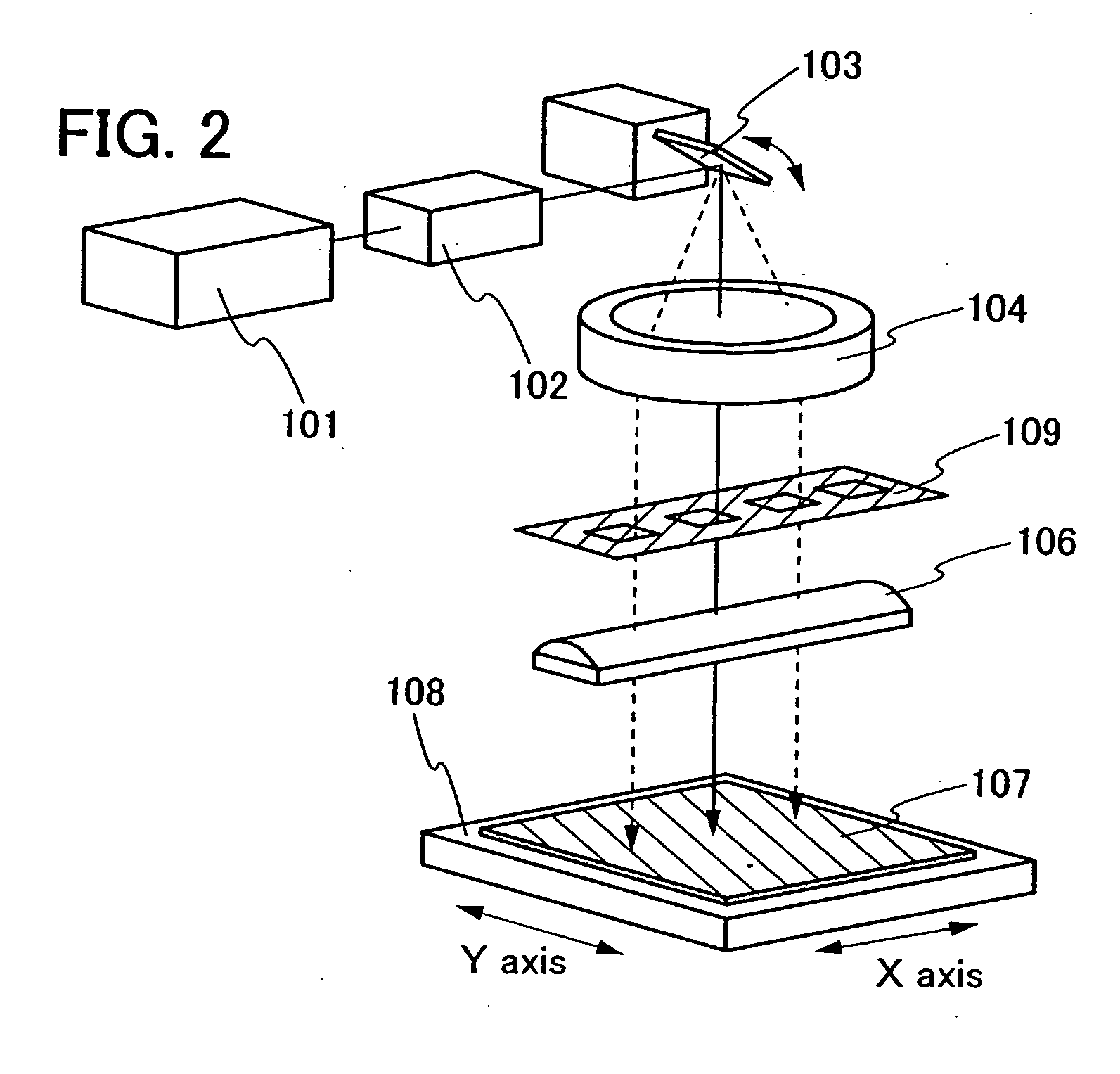
[0092] Embodiment 3 will describe an example of projecting an image at a slit opening portion onto an irradiation surface by changing the shape of slits disposed between an f-θ lens and the irradiation surface in accordance with the incidence angle of a laser beam.
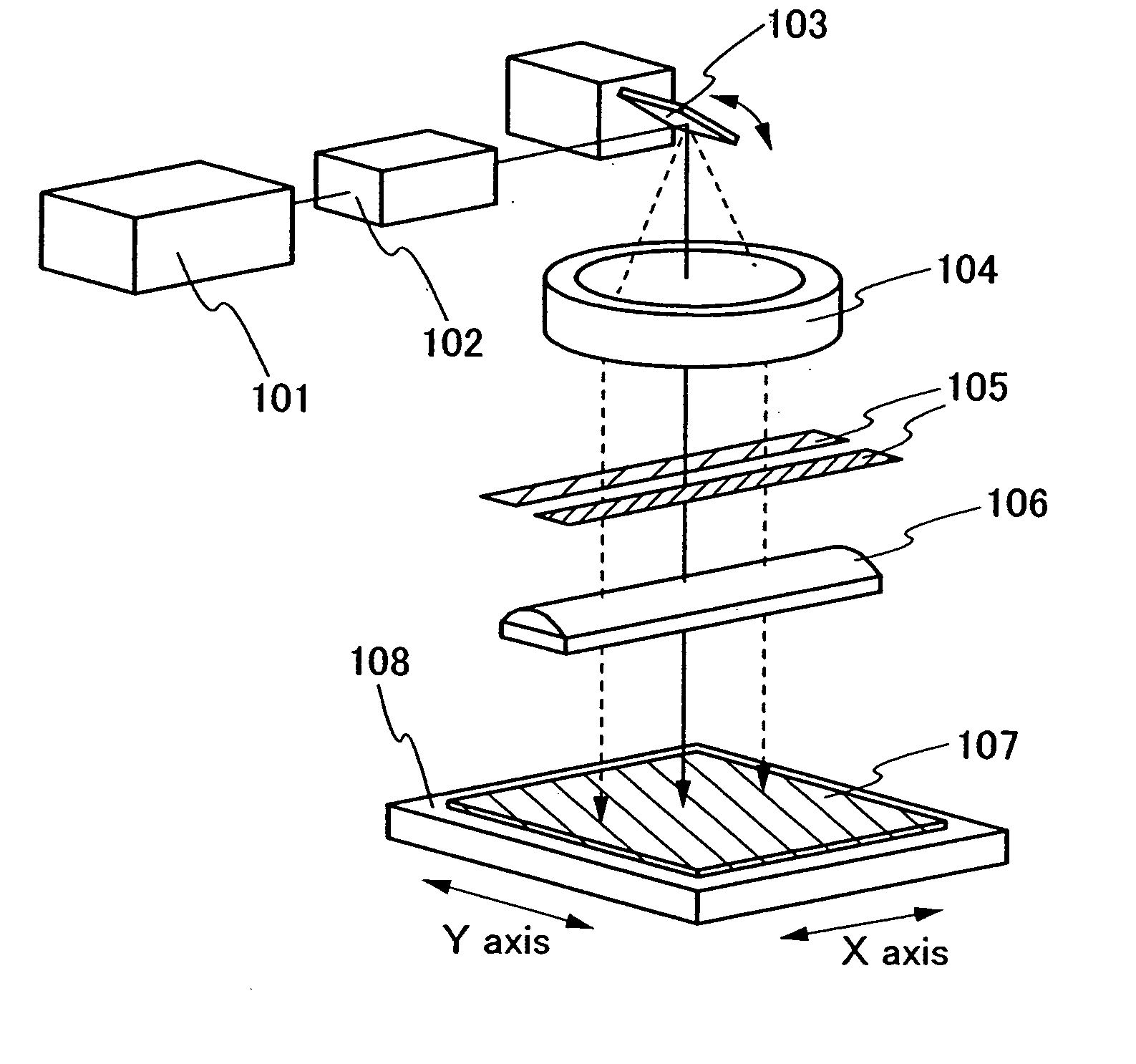
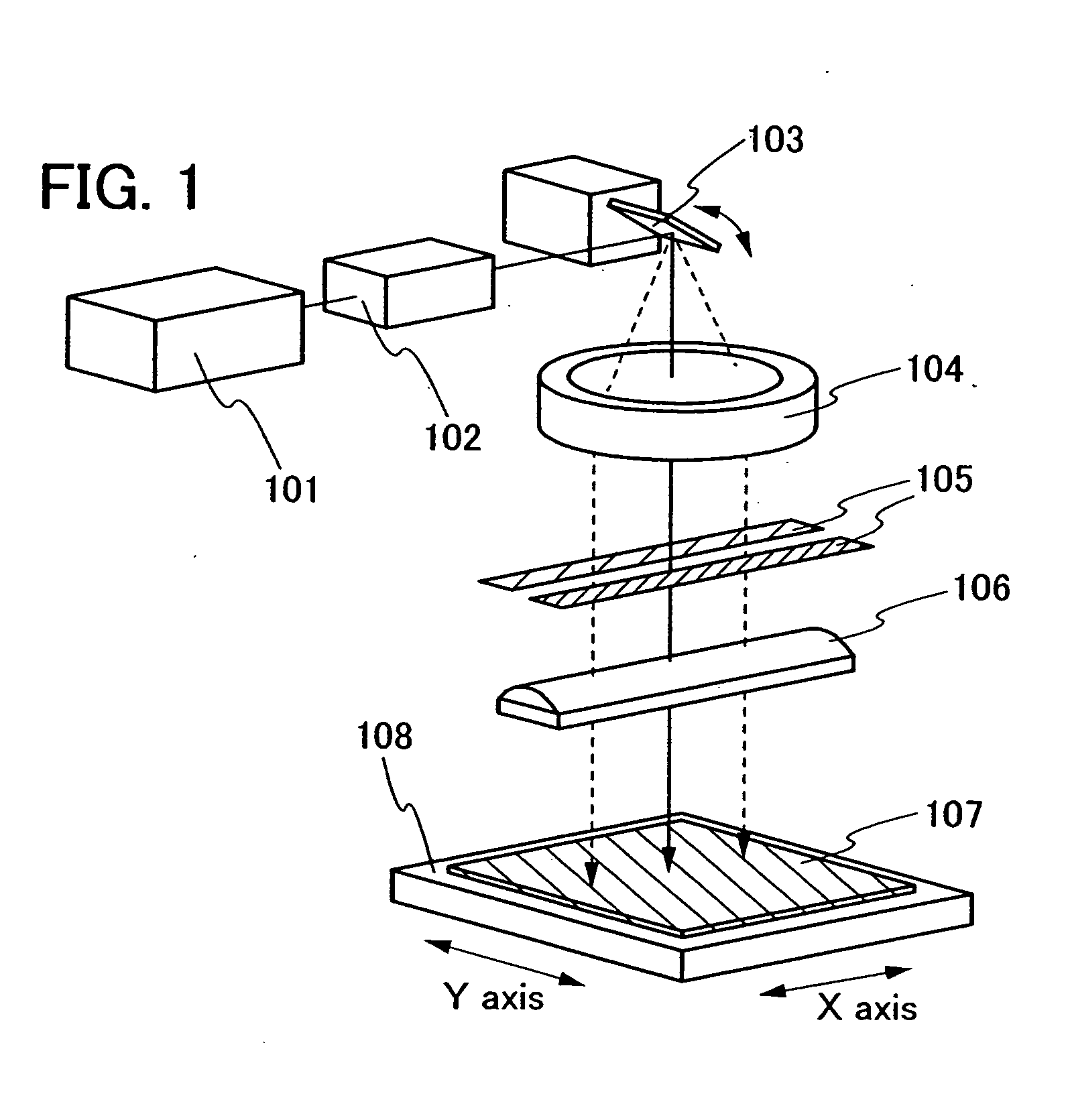
[0093]FIGS. 12A and 12B show an example of the above-described optical system. A laser beam emitted from a laser oscillator enters a galvanometer mirror 601. The galvanometer mirror 601 has a function of deflecting a laser beam, and the irradiation surface can be scanned with the laser beam by changing the angle of inclination of the galvanometer mirror 601. The laser beam deflected by the galvanometer mirror 601 is condensed to an irradiation surface 605 by an f-θ lens 602 including two spherical lenses 602a and 602b. Both edges of a beam spot in a main-axis direction, of the laser beam having passed through the f-θ lens 602 are removed by a slit 603.
[0094] The slit 603 is disposed so as to be curved as shown in FIG. 12...
PUM
| Property | Measurement | Unit |
|---|---|---|
| length | aaaaa | aaaaa |
| length | aaaaa | aaaaa |
| power | aaaaa | aaaaa |
Abstract
Description
Claims
Application Information