Semiconductor integrated circuit device

a technology of integrated circuits and semiconductors, applied in the direction of power consumption reduction, pulse technique, instruments, etc., can solve the problems of gate oxide films, inability to cut off or reduce the current of the control circuit for controlling this power switch, and leakage current flowing through these circuits when they are not operating, so as to and reduce the leakage current

Active Publication Date: 2007-06-21
RENESAS ELECTRONICS CORP
View PDF2 Cites 52 Cited by
  • Summary
  • Abstract
  • Description
  • Claims
  • Application Information

AI Technical Summary

Benefits of technology

[0013] Thus, the drive circuit, which cannot be turned off even when the circuit block is in its standby state, includes a double gate transistor (the first transistor) having an asymmetrical double gate structure (that is, having two gates with different gate insulating film thicknesses). With this arrangement, when the circuit block is not operating, the gate of the double gate transistor having a smaller gate insulating film thickness is turned off and that having a larger gate insulating film thickness is turned on to reduce the leakage current flowing through the gate insulating films while performing a required operation.
[0014] Thus, the present invention can reduce the leakage current of a control circuit provided to reduce the leakage current of an LSI circuit by use of a power switch.

Problems solved by technology

However, the above circuitry is disadvantageous in that controlling the power switch PSW so as to cut off power supply to the circuit block Logic requires that the nMOS transistor MN1 in the circuit DRV for generating the signal SWON be turned on to set the voltage of the signal SWON to a low level.
Incidentally, as the size of circuits on an LSI (Large Scale Integrated Circuit) chip has been increased, the leakage current flowing through these circuits when they are not operating has become a limiting factor in reducing the power consumption of the chip.
However, although it is possible to reduce the leakage current of these circuits connected to the power switch, it is not possible to cut off or reduce the current of the control circuit for controlling this power switch.
As fine processing technology for semiconductor devices has advanced, the thickness of the gate oxide films (i.e., gate insulating films) of transistors has been reduced, resulting in an increase in the gate leakage current flowing through these films.

Method used


Image

  • Semiconductor integrated circuit device
  • Semiconductor integrated circuit device
  • Semiconductor integrated circuit device

Examples


first embodiment

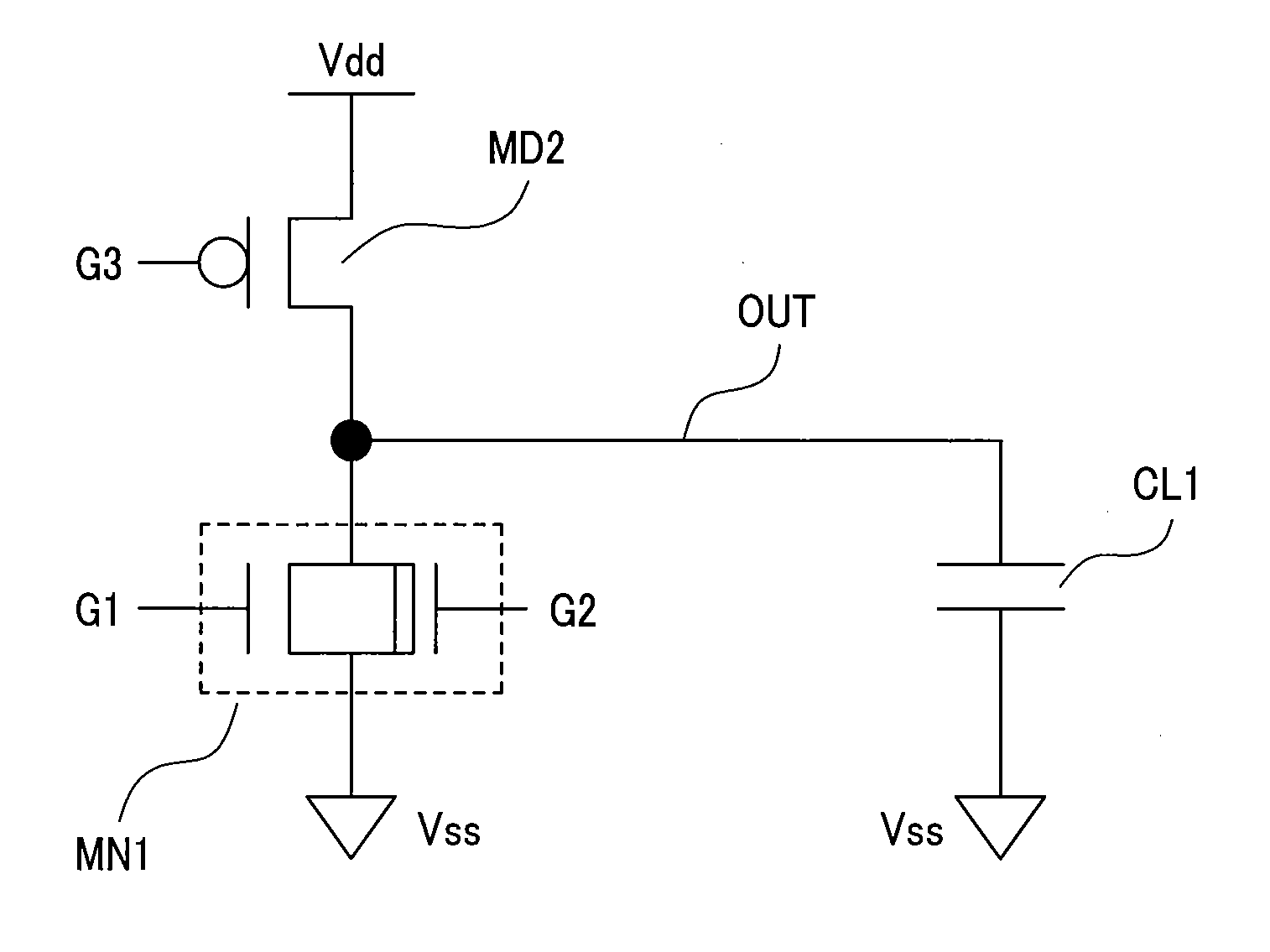
[0059]FIG. 1 shows a circuit diagram of a load driving circuit according to a first embodiment of the present invention. Referring to the figure, reference numeral MD1 denotes an n-channel double gate transistor for driving the load; MD2, a p-channel transistor for driving the load; OUT, a load node to be driven; CL1, the load, namely, a capacitor; G1, the first gate of the double gate transistor MD1; G2, the second gate of the double gate transistor MD1; G3, the gate of the transistor MD2; and Vss, a ground potential line.

[0060] The following preferred embodiments of the present invention assumes that circuits and circuitry employ a power supply voltage of 1.0 V, a high level voltage of 1.0 V, and a low level voltage of 0 V, unless otherwise stated. However, a power supply voltage other than 1.0 V, for example, 1.2 V or 0.8 V, may be used, with the same effect.

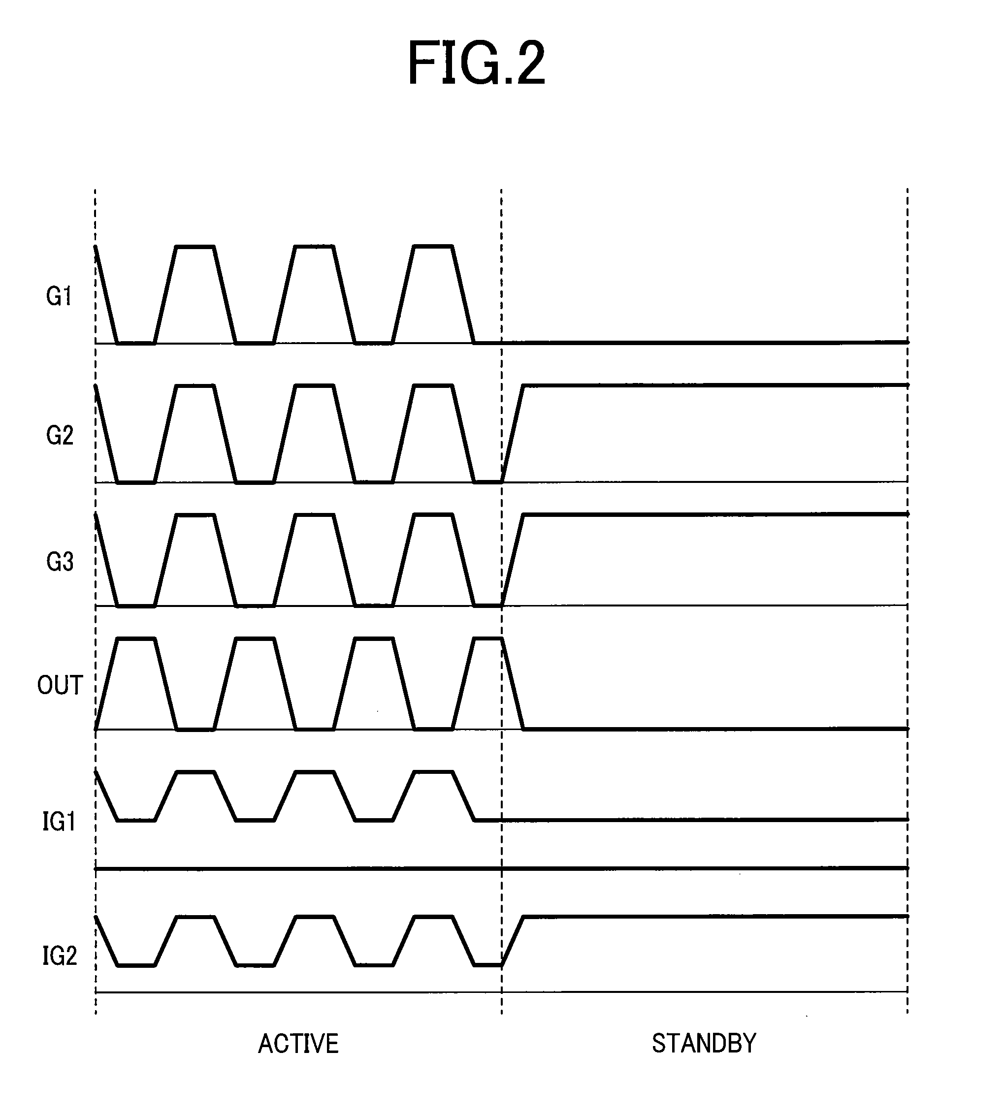
[0061]FIG. 2 shows the relationships between the voltages and currents at gates and nodes in the load driving circuit sho...

second embodiment

[0071]FIG. 7 shows a circuit diagram of leakage current reduction circuitry according to a second embodiment of the present invention. Referring to the figure, symbol Logic denotes an integrated circuit block including many circuits; Vssm, a ground potential line within the circuit block Logic; STBY, a standby signal, which is set at a high level when the circuit block Logic is in its standby state; PSW, a power switch used to cut off power supply to the circuit block Logic; SWON, a signal for controlling the power switch PSW; DRV, a drive circuit for generating the signal SWON (or driving the power switch PSW); SWEN, a signal for controlling the drive circuit DRV; and Ilogic, a current flowing through the circuit block Logic.

[0072]FIG. 8 shows changes in node (or signal) voltages and currents in the circuitry shown in FIG. 7. When the circuit block Logic is in the active state, the power switch PSW is turned on and hence the ground potential line Vssm is set to ground potential Vs...

third embodiment

[0075]FIG. 9 shows a circuit diagram of leakage current reduction circuitry according to a third embodiment of the present invention. Referring to the figure, symbol Logic denotes an integrated circuit block including many circuits; Vssm, a ground potential line within the circuit block Logic; STBY, a standby signal, which is set at a high level when the circuit block Logic is in its standby state; PSW, a power switch made up of a double gate transistor and used to cut off power supply to the circuit block Logic; SWON1, a signal for controlling the first gate of the power switch PSW (made up of the double gate transistor); SWON2, a signal for controlling the second gate of the power switch PSW (made up of the double gate transistor); DRV, a drive circuit for generating the control signals SWON1 and SWON2 (or driving the power switch PSW); SWEN, a signal for controlling the drive circuit DRV; and Inoise, the current flowing from the power switch PSW to a ground potential line Vss. It...


PUM


Abstract

An object of the present invention is to provide a technique of reducing the leakage current of a drive circuit for driving a circuit that must retain a potential (or information) when in its standby state. A semiconductor integrated circuit device of the present invention includes a drive circuit for driving a circuit block. This drive circuit is made up of a double gate transistor with gates having different gate oxide film thicknesses. When the circuit block is in its standby state, the gate of the double gate transistor having a thinner gate oxide film is turned off and that having a thicker gate oxide film is turned on. This arrangement allows a reduction in the leakage currents of both the circuit block and the drive circuit while allowing the drive circuit to deliver or cut off power to the circuit block.

Description

CLAIM OF PRIORITY [0001] The present application claims priority from Japanese application JP 2005-366784, filed on Dec. 20, 2005, the content of which is hereby incorporated by reference into this application. BACKGROUND OF THE INVENTION [0002] 1. Field of the Invention [0003] The present invention relates to a semiconductor integrated circuit device in which a processing circuit is integrated on a semiconductor chip to perform specific processing on a received signal and output the processed signal, and more particularly to a technique of reducing the power consumption of such a semiconductor integrated circuit device. [0004] 2. Description of the Related Art [0005] An exemplary conventional circuit for reducing the leakage current of a logic circuit includes an n-channel transistor and an inverter circuit. The n-channel transistor operates as a switch for cutting off power supply to the logic circuit, and the inverter circuit is used to drive the n-channel transistor. (See, for e...

Claims


Application Information

Patent Timeline
Patent Type & Authority Applications(United States)
IPC IPC(8): H03K19/003
CPCG11C11/413H03K19/0016
Inventor YAMAOKA, MASANAOKAWAHARA, TAKAYUKI
Owner RENESAS ELECTRONICS CORP
Why Eureka
Try Eureka