Oscillation circuit and a semiconductor circuit device having the oscillation circuit

a technology of oscillation circuit and oscillation circuit, which is applied in the direction of oscillator, electrical apparatus, etc., can solve the problems of chip size, number of external parts, and inability to meet the frequency range required by wcdma cellular phones, and achieve the effect of reducing chip size and small variation of q

Inactive Publication Date: 2007-06-28
RENESAS TECH CORP
View PDF2 Cites 42 Cited by
  • Summary
  • Abstract
  • Description
  • Claims
  • Application Information

AI Technical Summary

Benefits of technology

[0020] That is, according to the invention, it is possible to realize an LC resonance type oscillation circuit with a wide frequency variable range with a small variation ...

Problems solved by technology

The VCO having been put into practical use was not the one that can sufficiently meet the frequency range required by the WCDMA cellular phone.
Not only the reduction of the chip size of the IC but also the reduction of the number of external parts and ...

Method used


Image

  • Oscillation circuit and a semiconductor circuit device having the oscillation circuit
  • Oscillation circuit and a semiconductor circuit device having the oscillation circuit
  • Oscillation circuit and a semiconductor circuit device having the oscillation circuit

Examples


first embodiment

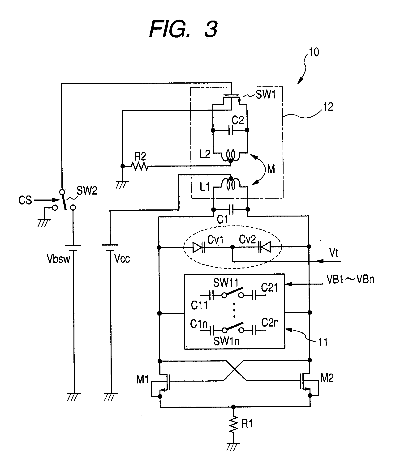
[0035]FIG. 3 shows a voltage controlled oscillator (VCO) according to the invention. All elements constituting a circuit of this embodiment are on-chip elements. The VCO is formed as a semiconductor circuit device over a single semiconductor chip such as single-crystal silicon.

[0036] In the embodiment, a VCO 10 is a resonance type oscillation circuit having a pair of n-channel MOSFETs (Metal Oxide Semiconductor Field Effect Transistors) M1, M2 as negative resistances. The MOSFETs M1, M2 are connected to a common source and their gates and drains are cross connected to each other. A resistance R1 is connected between the common source of the MOSFETs M1, M2 and a ground point GND. Between the drains of the MOSFET M1, M2, variable capacitance elements Cv1, Cv2 including a capacitance array 11 and a varactor diode, a fixed capacitance C1, and an inductor L1 are connected in parallel to each other. A power source voltage terminal Vcc is connected to an intermediate node of the inductor L...

fourth embodiment

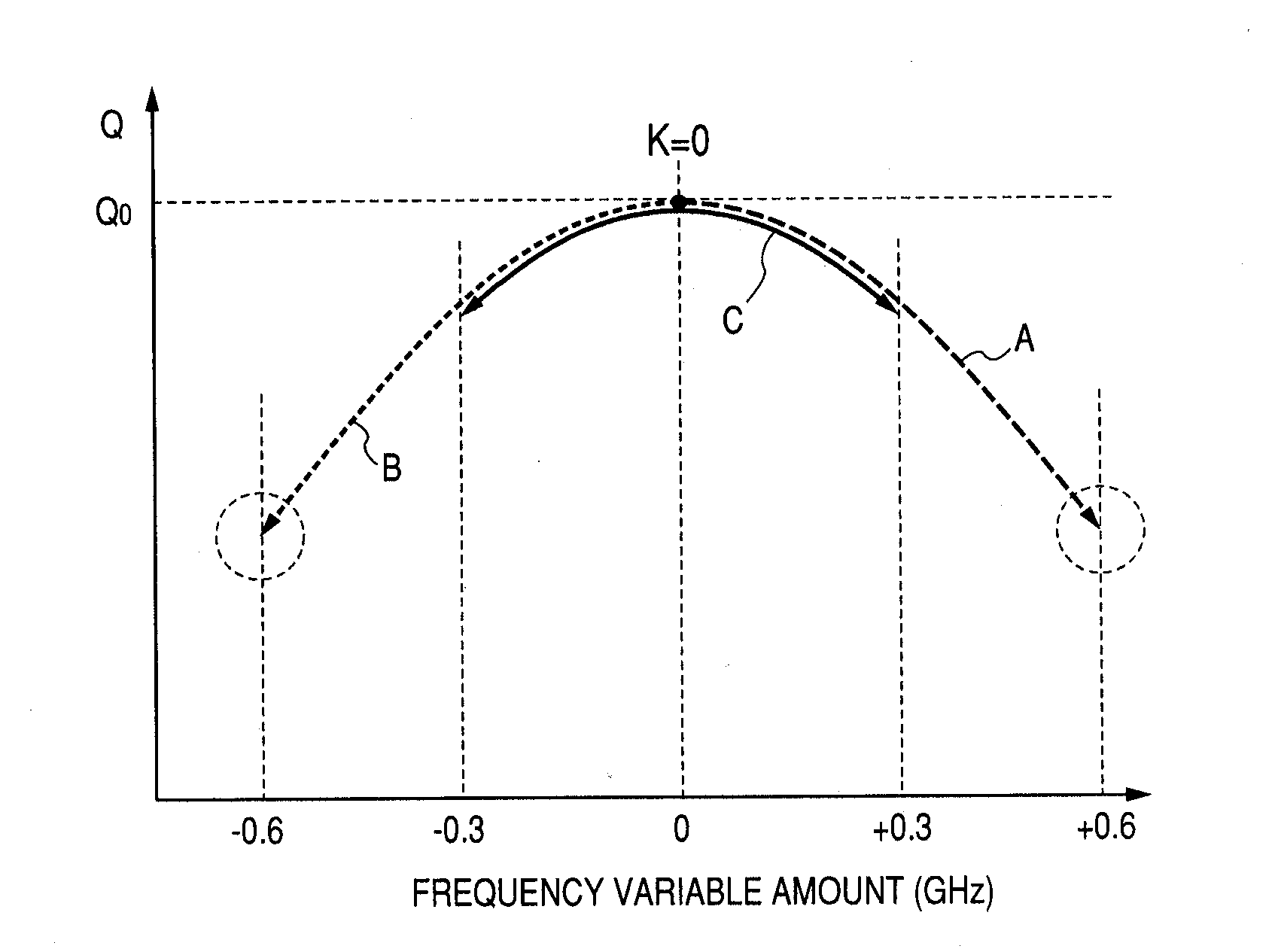
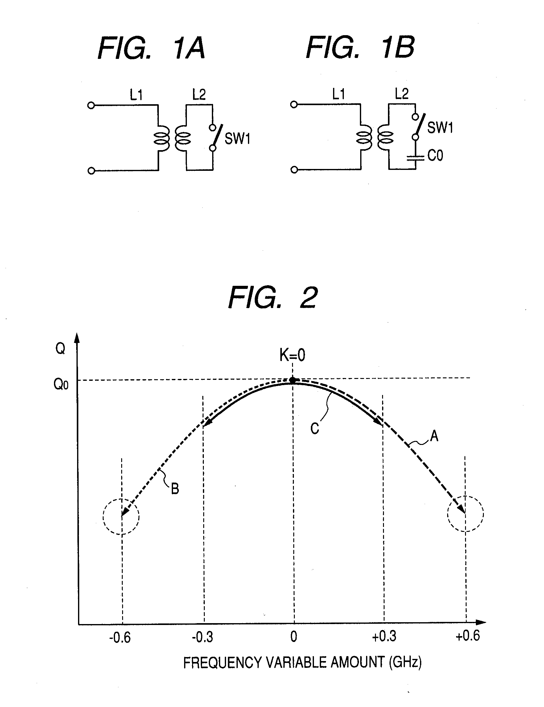
[0054]FIG. 9 shows the VCO according to the invention. The VCO of this embodiment is designed so that as the switch MOSFET SW1 constituting the variable inductance circuit 12, parasitic capacitances Cs1, Cs2 connected to the sources and drains are actively used as the capacitance elements connected to the both terminals of the secondary side inductor L2.

[0055] By using the parasitic capacitances of the respective sources and drains of the MOSFET SW1, the proper size of the capacitance element C2 connected between the both terminals of the secondary side inductor L2 can be reduced. Further, by increasing the size of the switch MOSFET SW1, the ON resistance can be reduced. With this feature, it is possible to avoid reducing the equivalent inductance value, namely, the variation amount of the VCO oscillation frequency due to the ON resistance of the SW1, by reducing the parasitic resistances serially connected to the secondary side inductor L2.

[0056] Here, as a method of increasing th...


PUM


Abstract

There is provided an LC resonance type oscillation circuit with a wide frequency variable range with a small variation of Q and capable of reducing a chip size due to no external parts required, and a communication semiconductor circuit device (high-frequency IC) having the oscillation circuit. In the LC resonance type oscillation circuit, a capacitance element and a switch element are connected in parallel between both terminals of a secondary side inductance element which is placed facing an inductance element constituting the LC resonance circuit and is connected by mutual induction to the inductance element. It is designed so that an equivalent inductance increases as the capacitance element is connected between the both terminals of the secondary side inductance element in a state where the switch element is turned OFF, and that the equivalent inductance decreases as the both terminals of the secondary side inductance element are short-circuited in a state where the switch element is turned ON.

Description

CROSS-REFERENCE TO RELATED APPLICATION [0001] The present application claims priority from Japanese patent application No. 2005-372705 filed on Dec. 26, 2005, the content of which is hereby incorporated by reference into this application. BACKGROUND OF THE INVENTION [0002] The present invention relates to a technology effectively applicable to a voltage controlled oscillator (VCO) and an LC resonance voltage controlled oscillator. It also relates to a technology effectively applicable to a voltage controlled oscillator included in a communication semiconductor circuit device constituting a wireless communication device, such as, for example, a cellular phone, to generate an oscillation signal of a wide frequency range used for modulation and demodulation of transmission and reception signals. [0003] In a wireless communication device such as a cellular phone, there is used a communication semiconductor circuit device (hereinafter referred to as a high-frequency IC) having a voltage ...

Claims


Application Information

Patent Timeline
IPC IPC(8): H03B5/08
CPCH03B2200/0048H03B2201/0216H03B2201/0266H03B5/1228H03B5/1268H03B5/1215H03B5/1243H03B5/1265
Inventor ARAI, IZUMIHORI, KAZUAKI
Owner RENESAS TECH CORP
Why Eureka
Try Eureka