Solar cell with superlattice structure and fabricating method thereof

a solar cell and superlattice technology, applied in the field of solar cells, can solve the problems of low energy conversion efficiency of silicon-based solar cells, poor light absorption of silicon solar cells, and material stacking, and achieve the effects of high carrier mobility, long diffusion length, and convenient storag

Inactive Publication Date: 2007-07-05
IND TECH RES INST +1
View PDF12 Cites 47 Cited by
  • Summary
  • Abstract
  • Description
  • Claims
  • Application Information

AI Technical Summary

Benefits of technology

[0017] In comparison with the prior, the present invention has preferable quality and advantages, such as high carrier mobility, long diffusion length, low trap density, and high efficiency of spectral response, so as to efficiently increase the growth critical thickness after crystallization.

Problems solved by technology

For a silicon-based solar cell, since silicon material is an indirect energy bandgap material, the light absorption of the silicon solar cell is poor and the energy conversion efficiency of the silicon-based solar cell is low, at most 24% or so at present.
However, this does not mean that any materials can be stacked together due to lattice matching.
When the difference among lattice constants of stacked materials is large, the strain will generate and to degrade the crystal quality.
That will lead to a crystalline defect, and further decrease the conversion efficiency of the solar cell.
Thus, the efficiency of conventional triple junction solar cell cannot be optimized.
However, in practice, since the quality of the InGaNAs material is rapidly deteriorated with the increase of the content of N, such that the carrier lifetime becomes shorter.
Therefore, it is very difficult to obtain an InGaNAs (1.0eV) epitaxy material with high quality, such that the structure still cannot be brought into practice at present.
However, many III-V semiconductor materials have lattice constants matching with GaAs and Ge, such as AlGaAs, GaInAs, GaInAsN, GaInP, and GaAsN, but each kind of those materials must be carefully prepared to stack because not all arbitrary combinations can completely match.
Therefore, the application region is small and the selection of materials for epitaxy growth is limited.
Furthermore, because it is difficult to match the lattices of conventional materials, stain is easily generated among the layers in the solar cell structure, such that a thicker epitaxy film cannot obtain, and the absorption region in the solar cell structure is limited, and further the efficiency of the solar cell is often negatively affected.
But the crystal quality of the material is poor, resulting in disadvantages such as shorter carrier diffusion length, lower mobility, shorter lifetime, and higher impurities concentration.
As a result, the efficiency of the whole solar cell cannot be enhanced efficiently.
In U.S. Pat. Nos. 4,688,068, 6,147,296, and 6,372,980, though quantum wells used in the multi-junction structure is claimed, the strain in the quantum well still cannot be completely compensated, such that the critical thickness in the crystal growing is thin or lattice defects are easily generated by the mismatching of lattices, which both negatively affect the conversion efficiency of the solar cell finally.

Method used


Image

  • Solar cell with superlattice structure and fabricating method thereof
  • Solar cell with superlattice structure and fabricating method thereof
  • Solar cell with superlattice structure and fabricating method thereof

Examples


Embodiment Construction

[0022] Specific embodiments will be provided to illustrate the content of the present invention in detail with reference to drawings. The symbols mentioned in the specification correspond to the symbols in the figures.

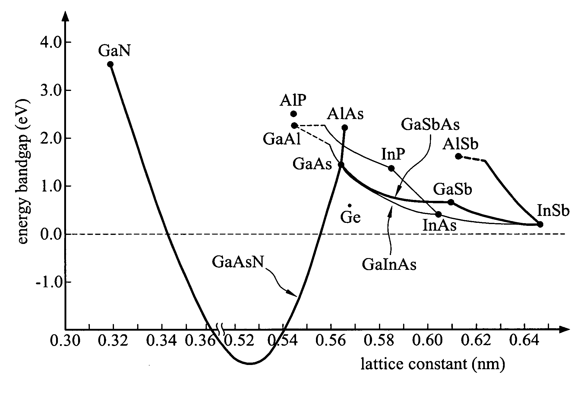
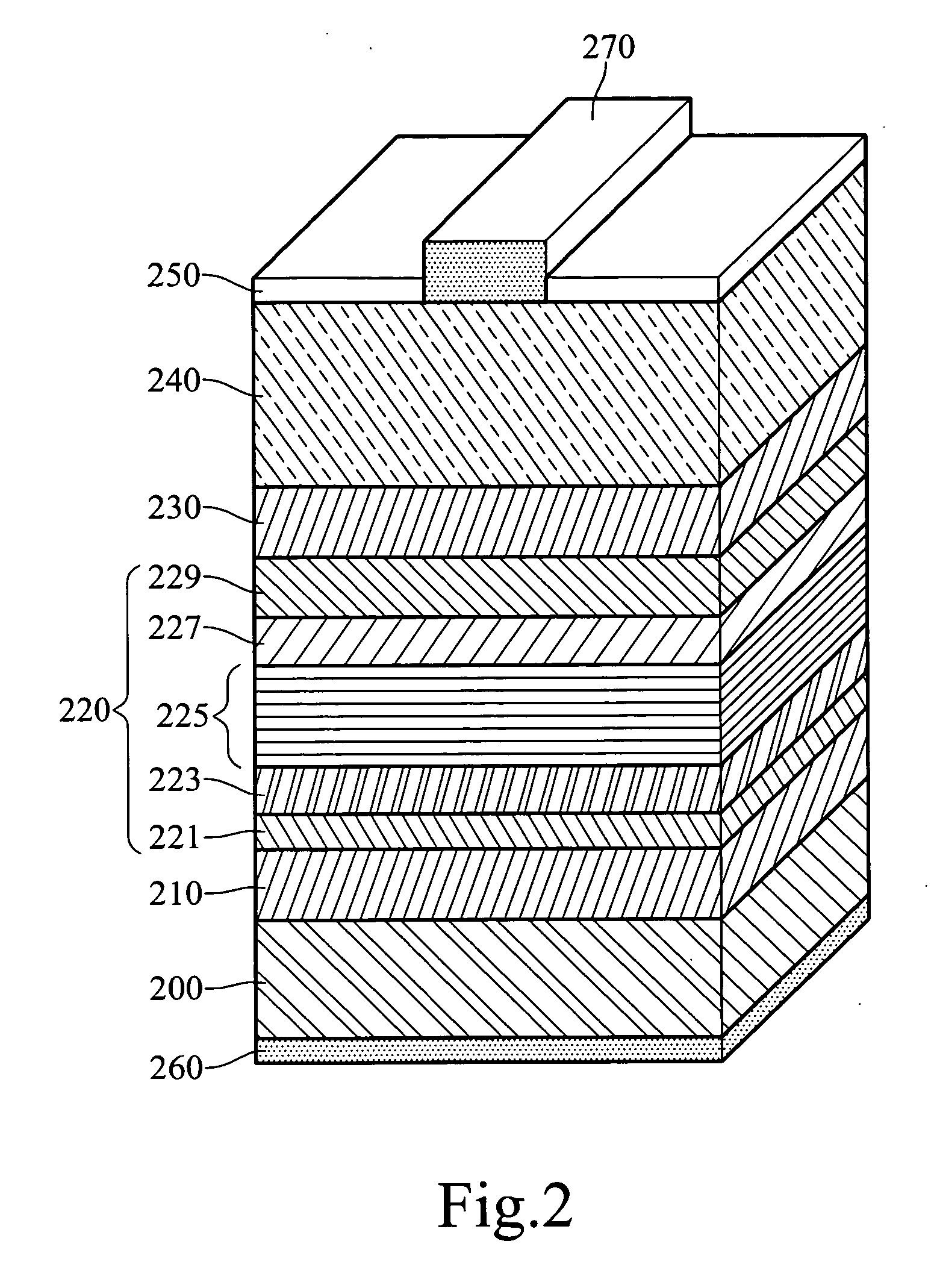
[0023] The present invention provides a solar cell with a superlattice structure, which includes a superlattice structure between the base and the emitter of the middle cell of the triple junction solar cell.

[0024] The aforementioned superlattice structure is, for example, a GaAsN / GaInAs superlattice structure, a GaAsN / GaSbAs superlattice structure, or a GaAsN / GaInSbAs superlattice structure.

[0025] When the aforementioned triple junction solar cell is, for example, a GaInP / GaAs / Ge, an AlGaAs / GaAs / Ge, an AlGaInP / GaAs / Ge, a GaInP / GaInAs / Ge, an AlGaAs / GaInAs / Ge, or an AlGaInP / GaInAs / Ge triple junction solar cell, the middle cell is a GaAs or a GaInAs middle cell. The base of the middle cell is a p-type or n-type GaAs, or a p-type or n-type GaInAs. The emitter is a p-ty...


PUM


Abstract

A solar cell with a superlattice structure and a fabricating method thereof are provided, which includes fabricating a superlattice structure of GaAsN / GaInAs, GaAsN / GaSbAs, or GaAsN / GaInSbAs between a base and an emitter of a middle cell of a triple junction solar cell by a strain-compensation technology. The provided solar cell not only decreases crystalline defects and increases the critical thickness of the crystal, but also makes the energy bandgap of GaAsN and GaInAs reach around the energy of 1.0 eV (electron volt). Hence, the absorption region can be raised to around the energy of 1.0 eV to enhance the efficiency of the solar cell.

Description

CROSS-REFERENCE TO RELATED APPLICATIONS [0001] This non-provisional application claims priority under 35 U.S.C. § 119(a) on Patent Application Ser. Nos. 094147747 filed in Taiwan, R.O.C. on Dec. 30, 2005, the entire contents of which are hereby incorporated by reference. BACKGROUND OF THE INVENTION [0002] 1. Field of Invention [0003] The present invention relates to a solar cell, and more particularly, to a solar cell with a superlattice structure and a fabricating method thereof. [0004] 2. Related Art [0005] At present, the commercial solar cells according to the materials can be classified into the silicon and the III-V compound semiconductor solar cells. For a silicon-based solar cell, since silicon material is an indirect energy bandgap material, the light absorption of the silicon solar cell is poor and the energy conversion efficiency of the silicon-based solar cell is low, at most 24% or so at present. For a III-V compound semiconductor solar cell, since. the III-V group comp...

Claims


Application Information

Patent Timeline
Patent Type & Authority Applications(United States)
IPC IPC(8): H01L31/00
CPCB82Y20/00H01L31/03046Y02E10/544H01L31/0725H01L31/035236Y02E10/548
Inventor CHIOU, CHIH-HUNGWU, PEI-HSUANCHEN, SHANG-FUCHEN, I-LIANGHSU, JUNG-TSUNGTZENG, ANDREW-YEN C.WU, CHIH-HUNG
Owner IND TECH RES INST
Why Eureka
Try Eureka