Maintenance of photoresist adhesion on the surface of dielectric arcs for 90 NM feature sizes
a technology of photoresist and feature size, which is applied in the field of fabrication of semiconductor devices, can solve the problems of increasing the maintenance cost of the chamber in terms of throughput, increasing the force exerted against the photoresist wall, and increasing the cost of carbon particulate byproducts of the deposition process chamber cleaning. , to achieve the effect of reducing the force exerted against the photoresist wall, and reducing the foot print of the photoresist wall
- Summary
- Abstract
- Description
- Claims
- Application Information
AI Technical Summary
Benefits of technology
Problems solved by technology
Method used
Image
Examples
example embodiments
Example One
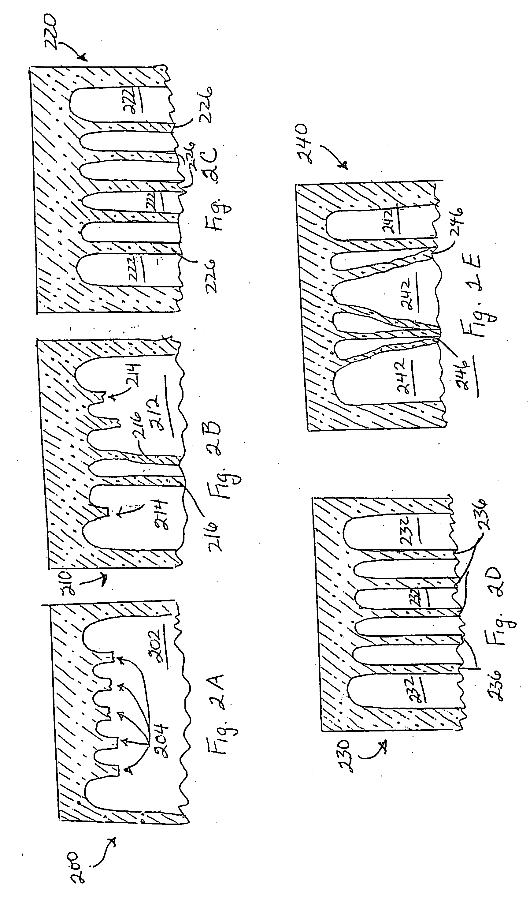
[0062] As a comparative example, a SiON DARC having an n (refractive index) of 1.9 and a k (extinction coefficient)of 0.3 @ 248 nm was capped with a 50 Å thick silicon oxide capping film generated from a SiH4 / CO2 / helium plasma using the general PECVD conditions of the kind described above for a single frequency plasma deposition process. The capped DARC exhibited a contact angle of 5.1 degrees with the water based alkaline developer used to develop the CAR, which was the SHIPLEY® UV6 photoresist. After exposure to either 230 J or 280 J of 248 nm patterning radiation, followed by development of the pattern, a photomicrograph of a top view 200 of the developed photoresist had the appearance illustrated by the schematic shown in FIG. 2A. The oxide-capped SiON DARC surface 202 was completely exposed in patterned areas after development of the photoresist, because the lines and spaces pattern which was to be developed failed due to detachment of the photoresist during develo...
example two
[0063] As a second comparative example, a nitrogen-free DARC 193 SiOxHy: C film having an n of 1.9 and a k of 0.3 @ 248 nm, which was surface treated with a CO2 plasma for a time period of about 20 seconds, using a CO2 flow rate of about 3 slm in a 200 mm PRODUCER® twin PECVD process chamber, using the single frequency plasma deposition process. The pressure was about 5 Torr, at a substrate temperature of about 350° C., at a plasma source power of about 50-100 W at 13.56 MHz, and at a shower head spacing of 450 mils from the substrate surface. The CO2-treated DARC 193, exhibited a contact angle of only 3.5 degrees with respect to the photoresist water-based alkaline developer. Exposure of the CAR to either 230 J or 280 J of 248 nm patterning radiation, and development of the imaged photoresist resulted in a developed photoresist where none of the patterned areas were present. All of the developed feature areas became detached from the DARC surface and washed away on development.
example three
[0064] As a third comparative example, a nitrogen-free DARC 193 SiOxHy: C film having an n of 1.9 and a k of 0.3 @ 248 nm, which was not surface treated, exhibited a contact angle of about 3.7 degrees with respect to the same developer mentioned with respect to Example Two. Exposure of the SHIPLEY® UV6 photoresist to 230 J of 248 nm patterning radiation, followed by development of the latent irradiated image in the photoresist, produced a relatively acceptable pattern. However, exposure of the CAR to 280 J of 248 nm patterning radiation, followed by development, produced a defective pattern in the CAR of the kind illustrated in FIG. 2B. FIG. 2B is a schematic top view 210 of a photomicrograph of the patterned photoresist. The DARC 193 surface 212 was exposed in some areas where the photoresist 216 should have been present. The photoresist 216 became detached, leaving broken off areas 214 where photoresist was missing. The difference in the developed pattern with such a slight differ...
PUM
| Property | Measurement | Unit |
|---|---|---|
| wavelength | aaaaa | aaaaa |
| sizes | aaaaa | aaaaa |
| radiation wavelength | aaaaa | aaaaa |
Abstract
Description
Claims
Application Information
 - R&D
- Intellectual Property
- Life Sciences
- Materials
- Tech Scout
- Unparalleled Data Quality
- Higher Quality Content
- 60% Fewer Hallucinations
Browse by: Latest US Patents, China's latest patents, Technical Efficacy Thesaurus, Application Domain, Technology Topic, Popular Technical Reports.
© 2025 PatSnap. All rights reserved.Legal|Privacy policy|Modern Slavery Act Transparency Statement|Sitemap|About US| Contact US: help@patsnap.com


