High density plasma non-stoichiometric SiOxNy films

a non-stoichiometric, high-density technology, applied in the direction of instruments, optical elements, plasma techniques, etc., can solve the problems of low plasma density, inefficient materials for optoelectronic devices, and inability to provide the wide range of optical dispersion characteristics required. , to achieve the effect of wide process margins and wide optical dispersion

Inactive Publication Date: 2007-07-05
SHARP KK
View PDF15 Cites 18 Cited by
  • Summary
  • Abstract
  • Description
  • Claims
  • Application Information

AI Technical Summary

Benefits of technology

[0025] The present invention describes a novel high-density plasma technique for the fabrication of stoichiometric, as well as non-stoichiometric SiOXNY (X+Y<2, and Y>0) thin films for novel optical devices. The HDP plasma processed SiOXNY thin-films may be embedded with nc-Si, and show a wide optical dispersion depending on the processing conditions. Like nc-Si embedded SiO2 films, it is possible to vary the refractive index (n) and the extinction constant (k) of nc-Si embedded SiOxNy thin-films in the range of 1.46-2.2 and 0-0.5, respectively, which overlaps the optical characteristics of various dielectric and semi conducting materials conventionally used for the fabrication of optical devices. In addition, the HDP plasma process enables the independent control of the n and k values, which can be successfully exploited for the fabrication of novel devices with wide process margins.

Problems solved by technology

While a single layer device would obviously be more desirable, no single thin-film material can provide the wide range of optical dispersion characteristics required to get the desired optical absorption, reflection, or transmission over a wide optical range extending from UV to far IR frequencies.
However, the indirect band-gap makes it an inefficient material for optoelectronic devices.
However, conventional PECVD and sputtering techniques have the limitations of low plasma density, inefficient power coupling to the plasma, low ion / neutral ratio, and uncontrolled bulk, and interface damage due to high ion bombardment energy.
Therefore, the oxide films formed from a conventional capacitively-coupled plasma (CCP) generated plasma may create reliability issues due to the high bombardment energy of the impinging ionic species.
However, it is not possible to control the ion energy using radio frequency (RF) of CCP generated plasma.
Any attempt to enhance the reaction kinetics by increasing the applied power results in increased bombardment of the deposited film, which creates a poor quality films with a high defect concentration.
Additionally, the low plasma density associated with these types of sources (˜1×10⁸-109 cm−3) leads to limited reaction possibilities in the plasma and on the film surface, inefficient generation of active radicals for enhanced process kinetics, inefficient oxidation, and reduction of impurities at low thermal budgets, which limits their usefulness in the fabrication of low-temperature electronic devices.
The higher temperature thermal processes can interfere with the other device layers and they are not suitable in terms of efficiency and thermal budget, due to the lower reactivity of the thermally activated species.

Method used


Image

  • High density plasma non-stoichiometric SiOxNy films
  • High density plasma non-stoichiometric SiOxNy films
  • High density plasma non-stoichiometric SiOxNy films

Examples


Embodiment Construction

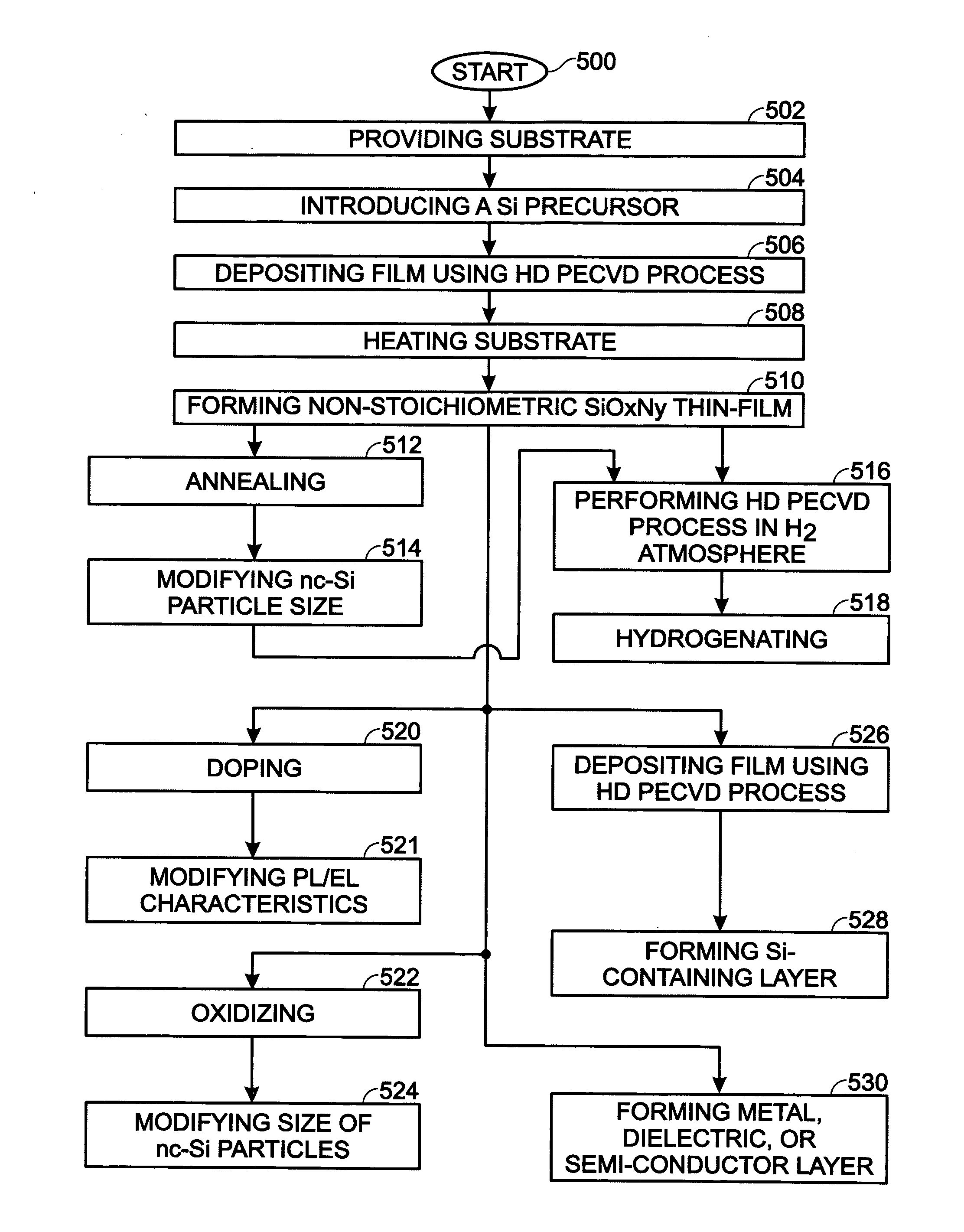
[0034] SiOXNY, both stoichiometric and Si rich (non-stoichiometric) films, can be fabricated using a high-density plasma (HDP) process, with many similarities to the processes previously presented in parent application Ser. No. 11 / 418,273. The process enables the fabrication of many possible device structure combinations, both single and multilayer, including the following materials: nc-Si embedded SiOx, SiNx, SiO2, Si3N4, and non-stoichiometric SiOXNY (X+YX or SiOXNY films can be fabricated under similar power / pressure range as described previously for SiOX films, however, the precursors are different.

[0035] A non-stoichiometric SiOXNY thin-film, as used herein, is understood to be a film with nanocrystalline (nc) Si particles, and may also be referred to as a Si-rich SiOXNY thin-film. The term “non-stoichiometric” as used herein retains the meaning conventionally understood in the art as a chemical compound with an elemental composition that cannot be represented by a ratio of we...


PUM

PropertyMeasurementUnit
temperatureaaaaaaaaaa
frequencyaaaaaaaaaa
pressureaaaaaaaaaa

Abstract

A high-density plasma method is provided for forming a SiOXNY thin-film. The method provides a substrate and introduces a silicon (Si) precursor. A thin-film is deposited overlying the substrate, using a high density (HD) plasma-enhanced chemical vapor deposition (PECVD) process. As a result, a SiOXNY thin-film is formed, where (X+Y<2 and Y>0). The SiOXNY thin-film can be stoichiometric or non-stoichiometric. The SiOXNY thin-film can be graded, meaning the values of X and Y vary with the thickness of the SiOXNY thin-film. Further, the process enables the in-situ deposition of a SiOXNY thin-film multilayer structure, where the different layers may be stoichiometric, non-stoichiometric, graded, and combinations of the above-mentioned types of SiOXNY thin-films.

Description

RELATED APPLICATIONS [0001] This application is a continuation-in-part of a pending patent application entitled, SILICON OXIDE THIN-FILMS WITH EMBEDDED NANOCRYSTALLINE SILICON, invented by Tingkai Li et al., Ser. No. 11 / 418,273, Attorney Docket No. SLA0963, filed May 4, 2006; [0002] which is a continuation-in-part of the following three pending patent applications: [0003] ENHANCED THIN-FILM OXIDATION PROCESS, invented by Pooran Joshi et al., Ser. No. 11 / 327,612, Attorney Docket No. SLA8012, filed Jan. 6, 2006; [0004] HIGH-DENSITY PLASMA OXIDATION FOR ENHANCED GATE OXIDE PERFORMANCE, invented by Joshi et al., Ser. No. 11 / 139,726, filed May 26, 2005, Attorney Docket No. SLA0944; and. [0005] HIGH-DENSITY PLASMA PROCESS FOR SILICON THIN-FILMS, invented by Pooran Joshi, Ser. No. 10 / 871,939, filed Jun. 17, 2004, Attorney Docket No, SLA0866; [0006] which is a continuation-in-part of the following three issued patents: [0007] METHOD FOR FABRICATING OXIDE THIN-FILMS, invented by Joshi et al....

Claims


Application Information

Patent Timeline
Patent Type & Authority Applications(United States)
IPC IPC(8): H01L21/20
CPCC23C16/308G02B1/10C23C16/509G02B1/11
Inventor JOSHI, POORAN CHANDRAVOUTSAS, APOSTOLOS T.HARTZELL, JOHN W.
Owner SHARP KK
Why Eureka
Try Eureka