ZnO nanostructure-based light emitting device

a light-emitting device and nano-structure technology, applied in the direction of nanotechnology, semiconductor devices, electrical equipment, etc., can solve the problems of high defect density of gan films for laser applications, difficult and high temperature deposition processes, and inability to obtain large-scale bulk crystals, etc., to improve light extraction, improve emission efficiency, and facilitate fabrication

Inactive Publication Date: 2007-07-12
RUTGERS THE STATE UNIV
View PDF4 Cites 55 Cited by
  • Summary
  • Abstract
  • Description
  • Claims
  • Application Information

AI Technical Summary

Benefits of technology

[0011] The present invention provides UV & blue Light Emitting Diodes (LEDs) based on zinc oxide (ZnO) nanostructures. In the present invention, the ZnO nanostructures grow on top of an existing GaN or ZnO LED as light extraction layer, or grow on top of a p-type GaN or ZnO layer to serve as an n-type layer to form nano-ZnO / GaN heterojunction LED or nanoZnO / epi-ZnO homojunction LED. In comparison with the conventional LEDs, the inventive ZnO nanostructured LEDs have improved emission efficiency. This results from the strong surface scattering which will randomize the angular distribution of photons inside the LED and an enlarged equivalent escape cone, leading to a high light extraction for the trapped photons. The dimension and aspect ratio of ZnO nanotips can be varies through control of growth conditions. The energy band, therefore transmission spectrum, can also be tuned by introducing dopants, such as Mg, to form MgxZn1−xO nanotips. Such ZnO nanostructured LEDs are easy to fabricate, are compact, and of low cost.
[0013] The present invention provides an LED, which is composed of n-type ZnO nanotips grown on p-type GaN film or p-type ZnO film. The n-type ZnO nanotips serve as the active layer in the p-n junction, and also as the extraction layer for high emission efficiency. The n-type ZnO nanotips can be grown on p-type GaN film, to form an n-type ZnO nanotips / p-GaN film heterojunction LED. The n-type ZnO nanotips can also be grown on p-type ZnO film, to form an n-type ZnO nanotips / p-ZnO film homojunction LED.
[0014] The present invention provides an LED, which consists of ZnO or MgxZn1−xO nanotips grown on a GaN p-n junction LED or on a ZnO p-n junction LED, in which ZnO nanotips serve as a passive layer to randomize the angular distribution of light emission and enhance the extraction efficiency.

Problems solved by technology

In spite of these developments, several challenges remain for GaN technology, such as a relatively high density of defects in GaN films for laser applications, difficult and high temperature deposition processes, non-availability of large size bulk crystals, and difficulty in wet chemical etching.
Furthermore, it is difficult to grow and pattern GaN nanostructures.
The main technical challenge remaining for nitride LEDs is the improvement of quantum efficiency.
Only ˜4% of the internal light can be extracted, which is limited by inherent loss, such as parasitic absorption during photon recyling and the narrow escape cone.
The difficulties in manipulating a GaN LED are due to its typically p-side-up structure, as Mg dopant has a memory effect, and p-GaN is usually high resistive and undesirable to grow thick.
However, laser lift off and Van der Waals bonding technologies are very complicated.
On the other hand, the employment of a tunneling junction could degrade the device's electrical and optical properties.
Despite these advantages, the development of ZnO based devices, such as LED, is still in the research stage, due to the difficulty in making a quality device using controllable and reproducible p-type doping.

Method used


Image

  • ZnO nanostructure-based light emitting device
  • ZnO nanostructure-based light emitting device
  • ZnO nanostructure-based light emitting device

Examples


Embodiment Construction

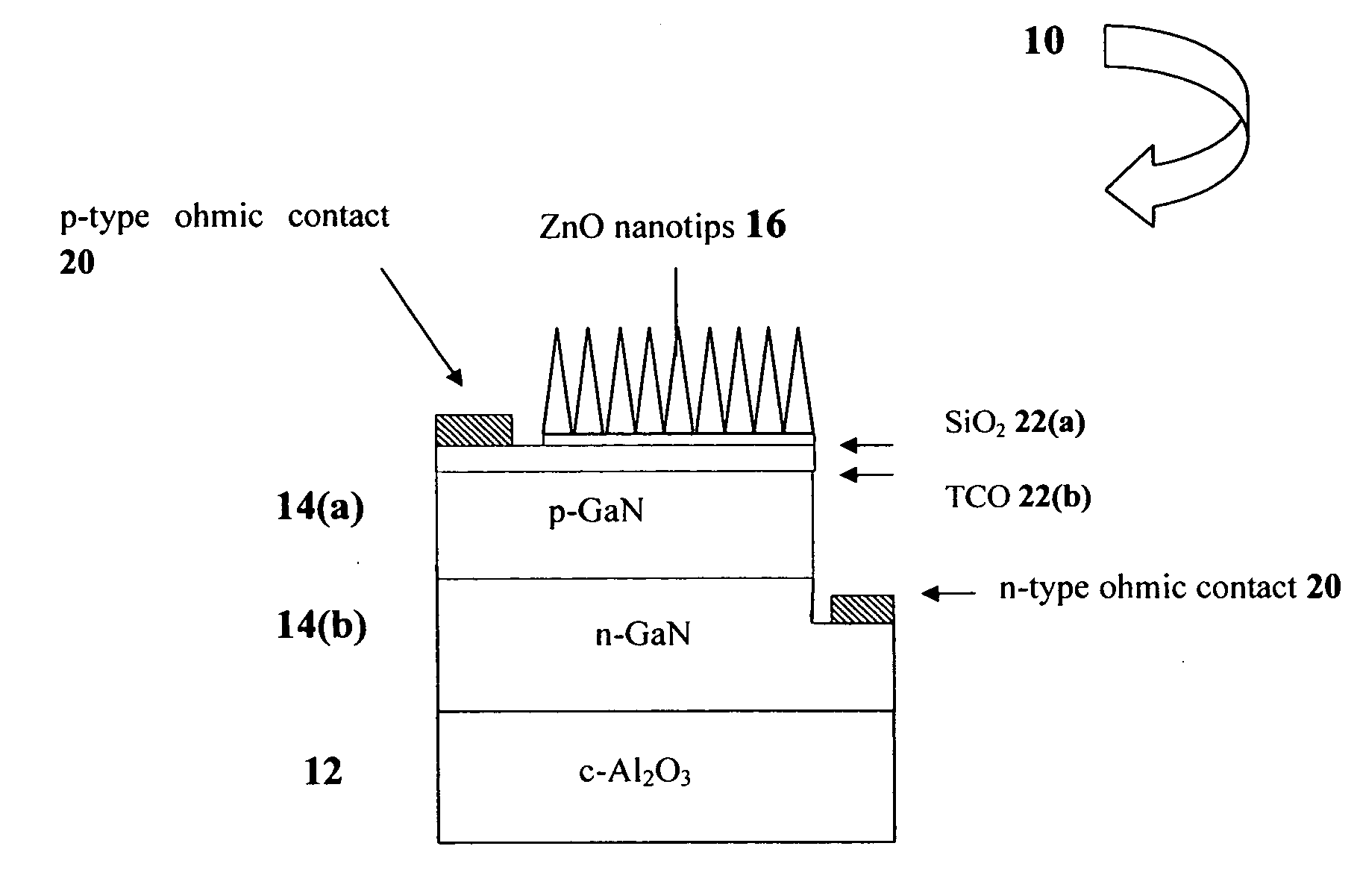
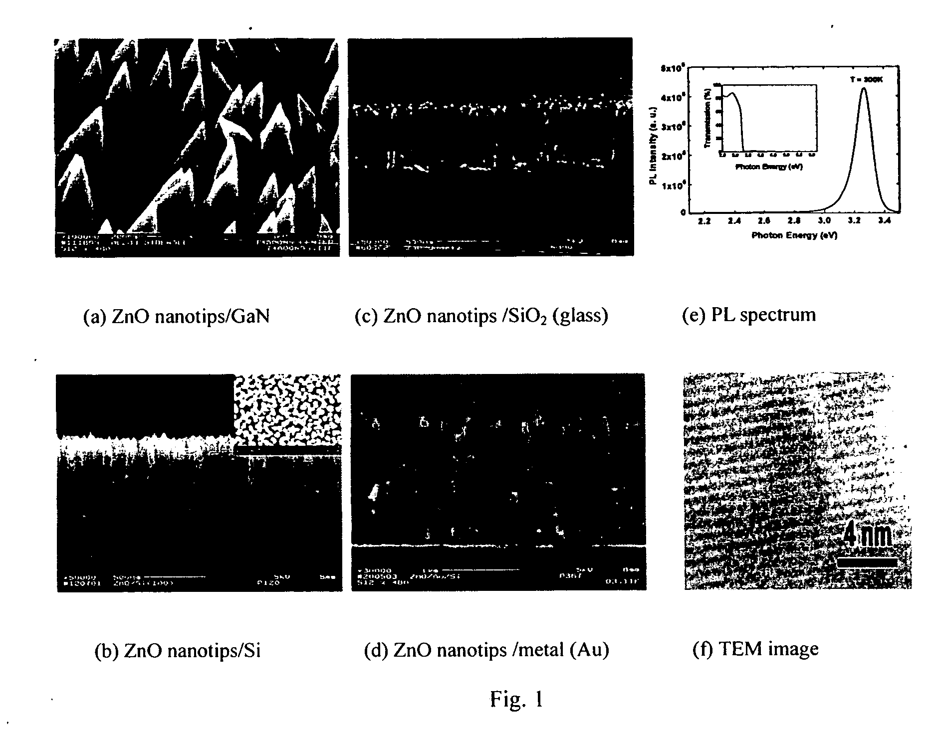
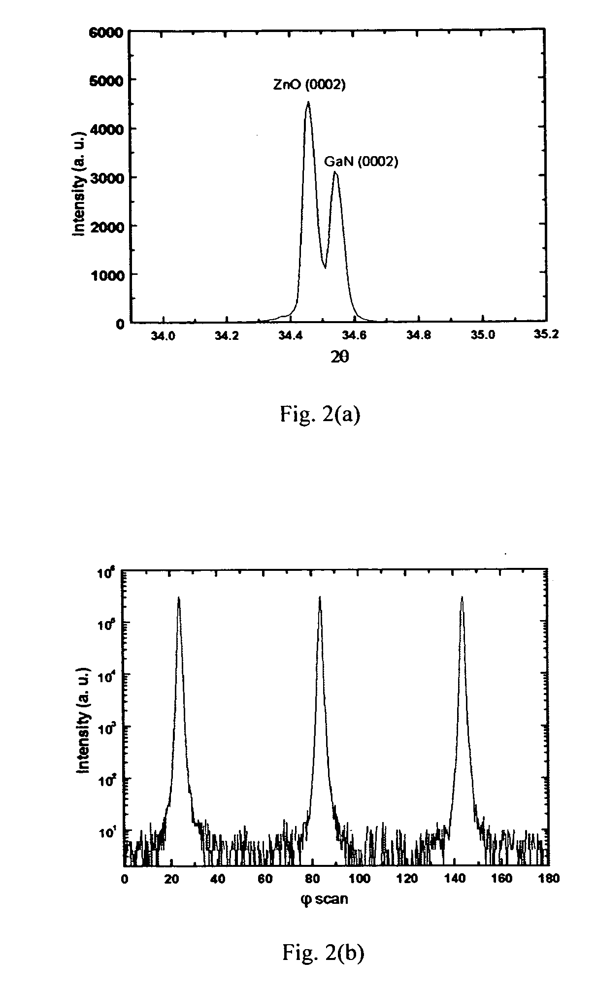
[0034] ZnO is an emerging direct wide bandgap semiconductor. ZnO is a polar semiconductor with the (0001) planes being Zn-terminated and the (000-1) planes being O-terminated. These two crystallographic planes have opposite polarity and hence have different surface relaxation energies. This leads to a higher growth rate along the c-axis. ZnO growth results in a pillar like structure called ZnO nanotips on these semiconducting, insulating and metallic substrates, while ZnO grown on R-plane sapphire substrates results in a smooth epitaxial film. The ZnO nanotips can be grown at relatively low temperatures, giving ZnO a unique advantage over other wide bandgap semiconductor nanostructures, such as GaN and SiC.

[0035] The ZnO nanostructure based light emitter is a compact UV / V is light emitter. Such a novel LED has many advantages over the broad area LED due to its unique material characteristics and device structure. In one type presented LED configuration, the active region utilizes n...


PUM


Abstract

ZnO nanostructure-based LEDs are provided to improve the emission efficiency. The devices include several configurations. Single crystal ZnO or MgxZn1−xO nanotips are grown on the top of a GaN p-n junction. Also, n-type ZnO nanotips are grown on p-GaN film to form an n-type ZnO nanotip / p-GaN heterojunction LED. A ZnO LED can be formed when depositing n-type ZnO nanotips on a p-type ZnO film layer. The ZnO nanotips, with a p-n junction in the tips, can be grown on glass for a low cost nano-LED, and can be grown on Si substrates to form an integrated ZnO nanoLED array on Si chips.

Description

[0001] This invention was made with partial Government support under Grant No. NSF CCR-0103096, awarded by the National Science Foundation. Therefore, the Government has certain rights in this invention.FIELD OF THE INVENTION [0002] This invention relates generally to Light Emitting Diode (LED) technology, and pertains more particularly to high quantum efficiency LEDs based on zinc oxide (ZnO) nanostructures for UV, blue, and white applications. BACKGROUND OF THE INVENTION [0003] UV / blue light emitting devices have a wide variety of military and civilian applications, including new solid light sources to save energy, non-line-of-sight (NLOS) covert communication, next-generation high-density optical storage, display, space communication, as well as biological and chemical detection. All require high efficient emitters. In particular, the higher the power intensity, the farther the NLOS transceivers can be placed apart. In a light emitting device, emission efficiency and low cost are...

Claims


Application Information

Patent Timeline
IPC IPC(8): H01L33/00H01L33/08H01L33/18H01L33/22H01L33/26H01L33/28
CPCB82Y20/00H01L21/02381H01L21/02458H01L21/02554H01L21/02565H01L33/28H01L33/08H01L33/18H01L33/22H01L33/26H01L21/0259
Inventor LU, YICHENGZHONG, JIAN
Owner RUTGERS THE STATE UNIV
Why Eureka
Try Eureka