Compound semiconductor, method of producing the same, and compound semiconductor device
- Summary
- Abstract
- Description
- Claims
- Application Information
AI Technical Summary
Benefits of technology
Problems solved by technology
Method used
Image

Examples
working examples
[0046] Although the present invention will be more concretely explained with reference to working examples in the following, the present invention is not limited to these working examples. While these working examples are set out taking a high electron mobility transistor (HEMT) as an example, similar application to a heterobipolar transistor (HBT) or p-i-n photodiode is possible. The growth method used in the working examples is the metalorganic chemical vapor deposition (MOCVD) method, but it is also possible to use the molecular beam epitaxy (MBE) method or the like. Although an InGaP buffer layer is taken by way of example in the working examples, an InGaAsP buffer layer can be similarly used.
example 1
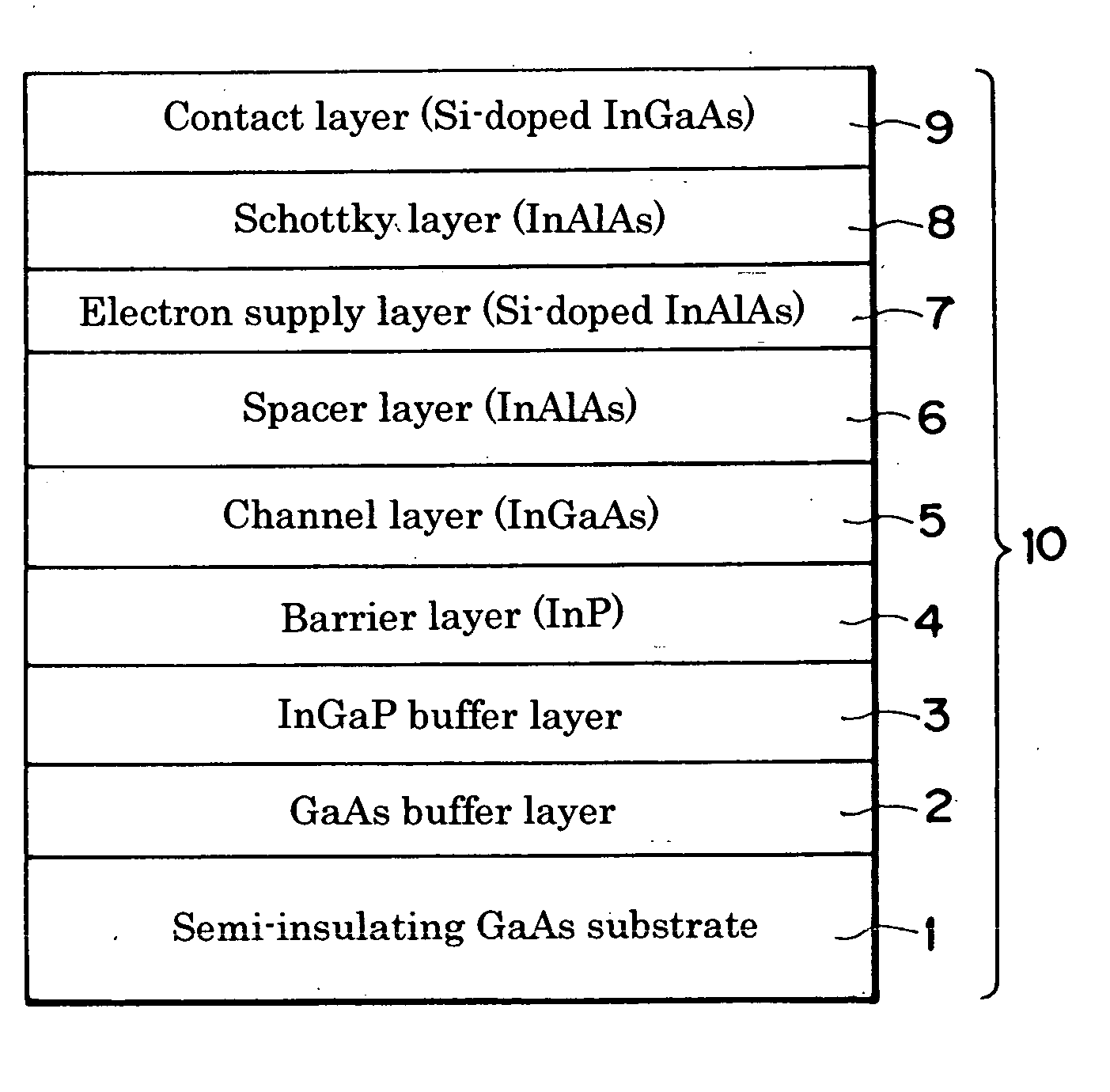
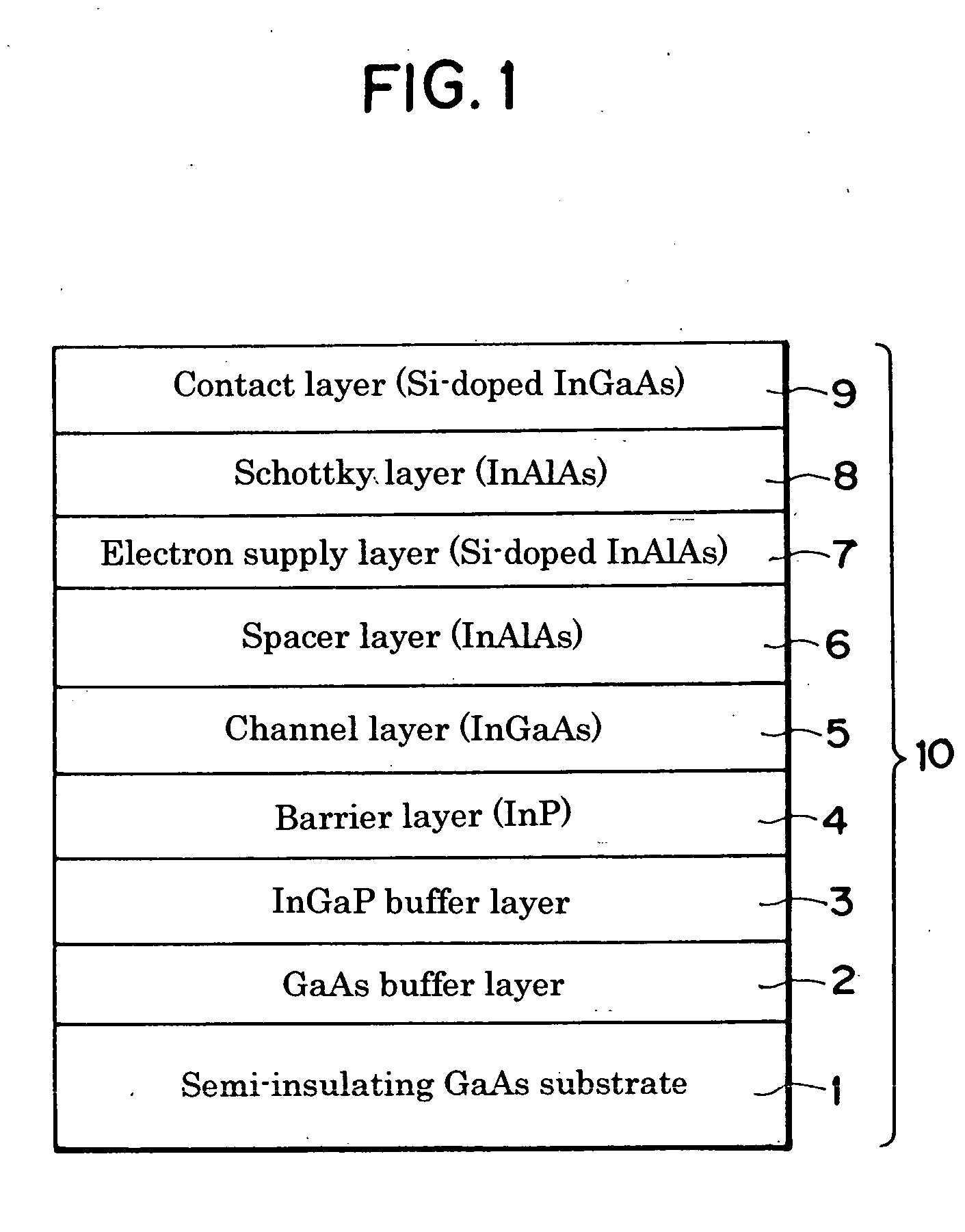
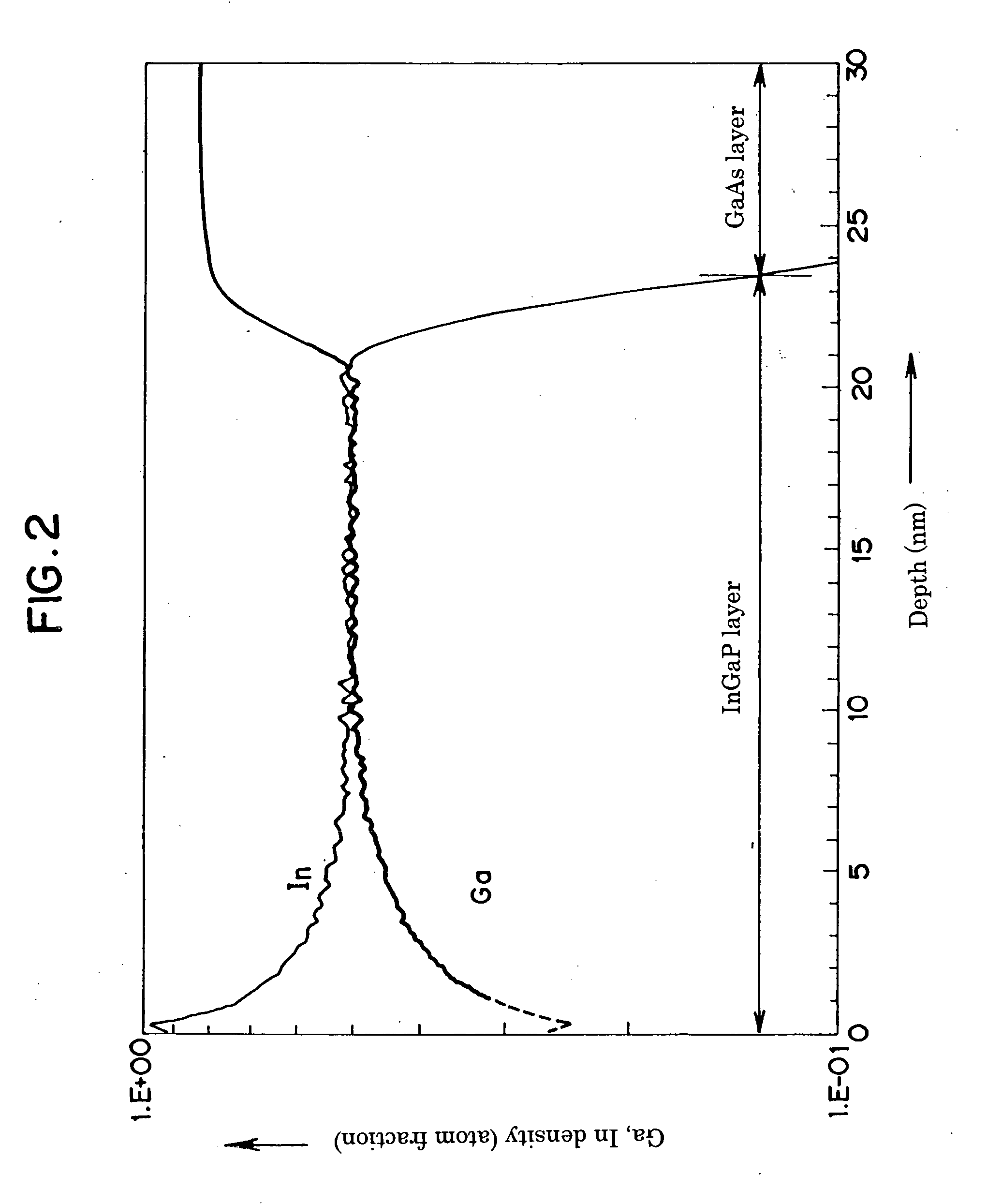
[0047] An HEMT epitaxial substrate having the compound semiconductor heterostructure of the layer structure shown in FIG. 1 was fabricated as follows using the MOCVD method. The semi-insulating GaAs substrate 1 was placed in a MOCVD film fabrication machine and elevated in temperature to conduct substrate surface treatment, whereafter the buffer layer 2 constituted as a GaAs layer was formed on the semi-insulating GaAs substrate using AsH3 gas and metalorganic compound as feedstock. Next, the AsH3 gas was switched to PH3 gas to form the InGaP buffer layer 3 (In content, 0.48) to a thickness of 30 nm. The InGaP buffer layer growth temperature at this time was 550° C. The temperature was suitably adjusted and the feedstock progressively changed to form in order the InP layer 4 (In content, 0.52), InGaAs channel layer 5 (In content, 0.53), InAlAs spacer layer 6 (In content, 0.52), electron supply layer (Si planar doped layer) 7, InAlAs Schottky layer 8 (In content, 0.52), and Si-doped ...
example 2
[0049] An HEMT epitaxial substrate was fabricated under exactly the same conditions as in Example 1 except that the InGaP buffer growth temperature was 500° C. and the thickness thereof was 15 nm. The surface condition of the obtained epitaxial substrate was excellent; absolutely no cloudiness, crosshatching or the like was observed.
[0050] The contact layer 9 of the epitaxial substrate was removed by etching and Hall measurement was performed at room temperature. The mobility of 8,900 cm2 / V·s exhibited was a value comparable to that of an HEMT epitaxial substrate using an InP substrate.
PUM
 Abstract
Description
Claims
Application Information
 - R&D
- Intellectual Property
- Life Sciences
- Materials
- Tech Scout
- Unparalleled Data Quality
- Higher Quality Content
- 60% Fewer Hallucinations
Browse by: Latest US Patents, China's latest patents, Technical Efficacy Thesaurus, Application Domain, Technology Topic, Popular Technical Reports.
© 2025 PatSnap. All rights reserved.Legal|Privacy policy|Modern Slavery Act Transparency Statement|Sitemap|About US| Contact US: help@patsnap.com