Method for manufacturing semiconductor device
a manufacturing method and semiconductor technology, applied in semiconductor devices, semiconductor/solid-state device testing/measurement, electrical equipment, etc., can solve problems such as signal delay due to wiring resistance, and achieve the effects of reducing contact resistance between source and drain electrode layers and oxide semiconductor layers containing in, ga, zn, and good electrical properties and reliability
- Summary
- Abstract
- Description
- Claims
- Application Information
AI Technical Summary
Benefits of technology
Problems solved by technology
Method used
Image

Examples
embodiment 1
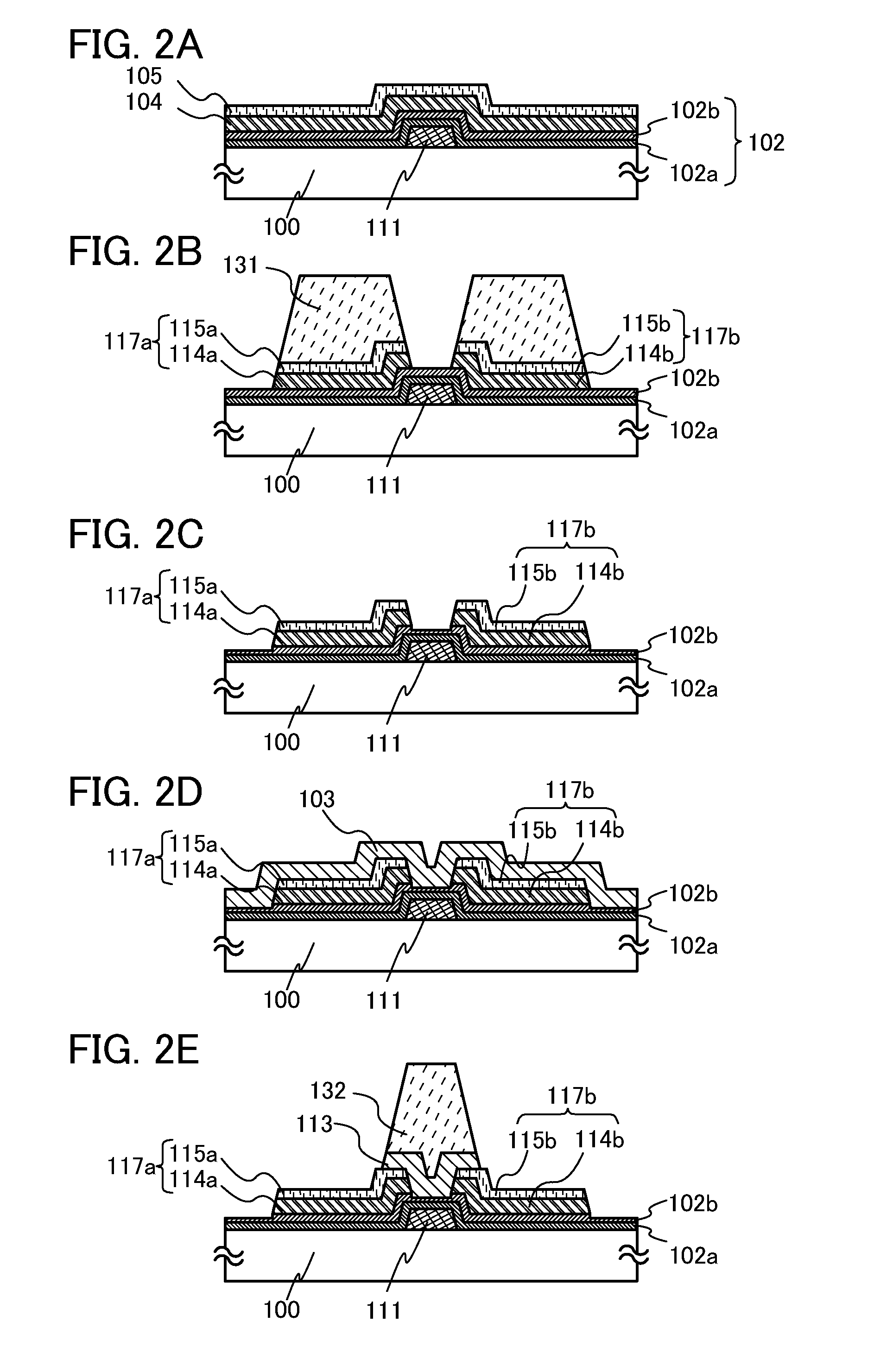
[0030]In this embodiment, a thin film transistor and a manufacturing process thereof will be described with reference to FIGS. 1A and 1B and FIGS. 2A to 2E.
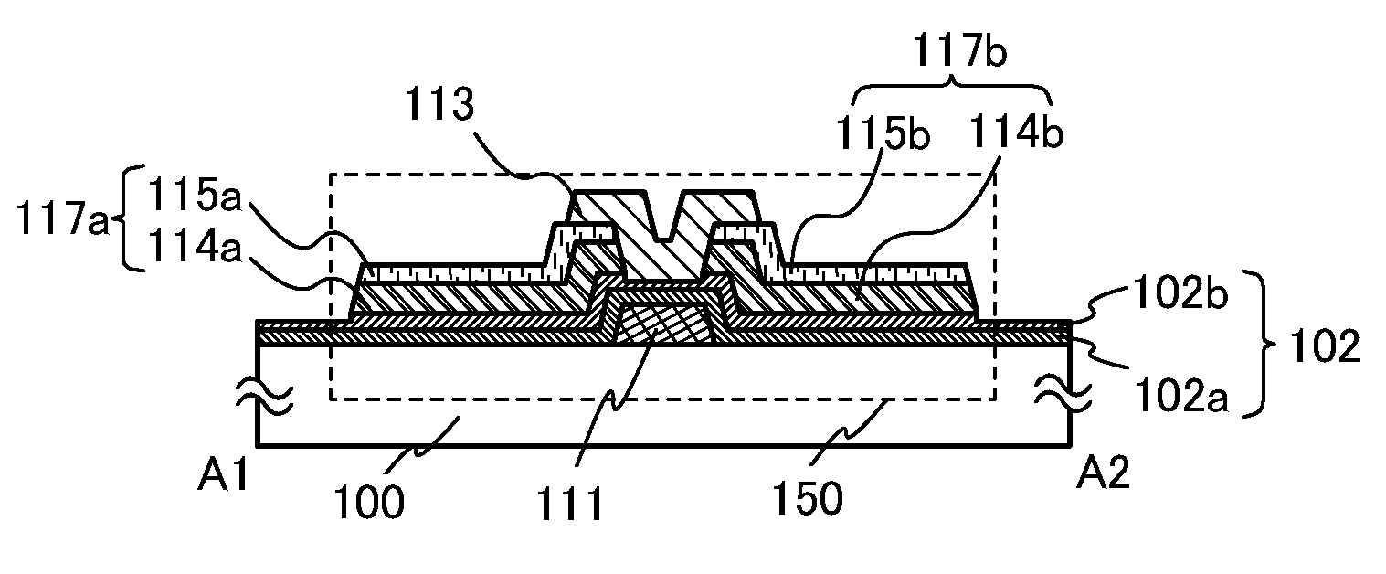
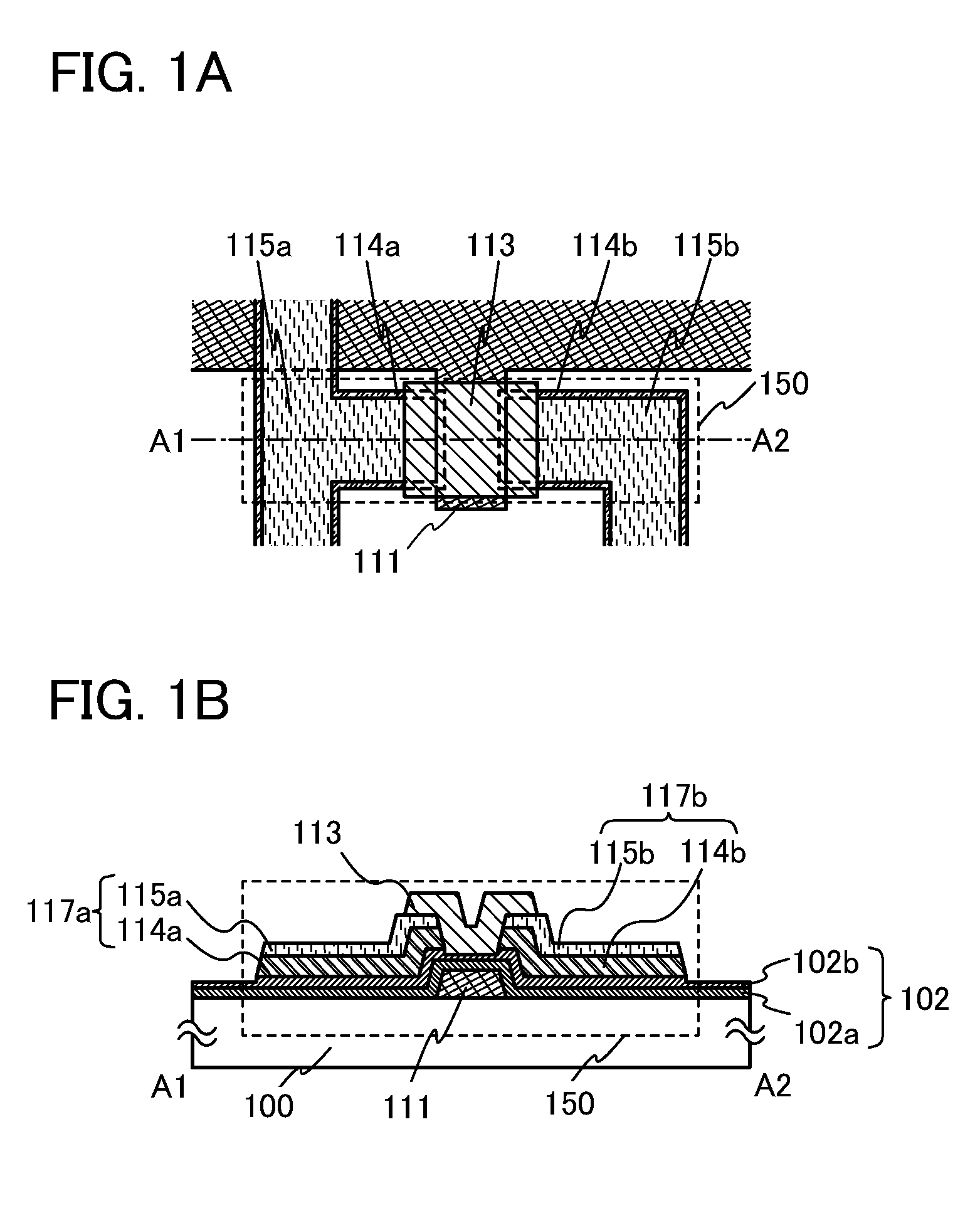
[0031]FIGS. 1A and 1B illustrate a bottom gate thin film transistor of this embodiment. FIG. 1A is a plan view and FIG. 1B is a cross-sectional view taken along line A1-A2 in FIG. 1A. In a thin film transistor 150 illustrated in FIGS. 1A and 1B, a gate electrode layer 111 is formed over a substrate 100, a gate insulating film 102 is formed over the gate electrode layer 111, source and drain electrode layers 117a and 117b are formed over the gate electrode layer 111 with the gate insulating film 102 interposed therebetween, and a semiconductor layer 113 which serves as a channel formation region is formed between the source and drain electrode layers 117a and 117b. Note that in this embodiment, the gate insulating film 102 includes two layers, a first gate insulating film 102a and a second gate insulating film 102b.
[0032]In FIG. ...
embodiment 2
[0080]In this embodiment, a thin film transistor mode of which is different from that in Embodiment 1 and a manufacturing process of the thin film transistor will be described with reference to FIG. 4 and FIGS. 5A to 5E. FIG. 4 is a cross-sectional view illustrating a staggered thin film transistor of this embodiment. In a thin film transistor 151 illustrated in FIG. 4, the source and drain electrode layers (117a and 117b) are formed over the substrate 100 and the semiconductor layer 113 is formed so as to cover the source and drain electrode layers (117a and 117b). A gate insulating layer 112 is formed over the semiconductor layer 113 and the gate electrode layer 111 is formed so as to overlap with the channel formation region with the gate insulating layer 112 interposed therebetween.
[0081]In FIG. 4, the source and drain electrode layers (117a and 117b) are formed using a high-melting-point metal material layer. Sputtering treatment with plasma is performed on the surfaces of the ...
example 1
[0107]In this example, a case where a bottom gate thin film transistor is manufactured by the method for manufacturing a semiconductor device which is described in Embodiment 1 will be described. Further, electrical properties of the thin film transistor are compared to those of a thin film transistor which is manufactured without performing plasma treatment on surfaces of source and drain electrode layers.
[0108]In this example, plasma treatment was performed on the surfaces of the source and drain electrode layers by a reverse sputtering method. The conditions of a reverse sputtering method were as follows: RF sputtering was performed with a pressure in a chamber of 0.4 Pa, a flow rate of an Ar gas of 50 sccm, and a power of 200 W.
[0109]The thin film transistor manufactured has a gate insulating film formed using a silicon oxynitride film with a thickness of 100 nm over a gate electrode layer formed using a tungsten film with a thickness of 100 nm; source and drain electrode layers...
PUM
 Abstract
Description
Claims
Application Information
 - R&D
- Intellectual Property
- Life Sciences
- Materials
- Tech Scout
- Unparalleled Data Quality
- Higher Quality Content
- 60% Fewer Hallucinations
Browse by: Latest US Patents, China's latest patents, Technical Efficacy Thesaurus, Application Domain, Technology Topic, Popular Technical Reports.
© 2025 PatSnap. All rights reserved.Legal|Privacy policy|Modern Slavery Act Transparency Statement|Sitemap|About US| Contact US: help@patsnap.com