Eureka AIR delivers breakthrough ideas for toughest innovation challenges, trusted by R&D personnel around the world.

Interdigitated capacitive structure for an integrated circuit

Active Publication Date: 2007-07-12
TAIWAN SEMICON MFG CO LTD
View PDF81 Cites 12 Cited by
  • Summary
  • Abstract
  • Description
  • Claims
  • Application Information

AI Technical Summary

Benefits of technology

[0014] An advantage of a preferred embodiment of the present invention is efficiently combining MOM and MIM-type capacitors. The layers of substantially parallel interdigitated strips can be configured similarly to existing MOM capacitors. The first dielectric layer and the first extension layer add MIM-type capacitance to the first layer of interdigitated strips. Thus, the MIM-type capacitor is sandwiched between layers of MOM capacitors, connected through vias.
[0015] A further advantage of a preferred embodiment of the present invention is reducing vertical chip area required for a desired capacitance per unit area. The addition of MIM-type capacitance between layers of a MOM capacitor adds surface area and extends the capacitive effect of one layer of MOM capacitor strips on the layer below it, between strips on the same layer, and between adjacent vias. Accordingly, the effective capacitance per unit area is increased, without additional process steps or expanding the vertical chip area required for a MOM capacitor.
[0016] Yet another advantage of a preferred embodiment of the present invention is improving mismatch performance. The addition of MIM-type capacitance between layers, coupled through vias to a layer above the MIM-type layer adds structural support that can offset mismatches in alignment between MOM capacitor strips. Further, the expanded capacitive field of the MIM-type layer and the associated vias improves the capacitive performance in the presence of mismatches in alignment between MOM capacitor strips.

Problems solved by technology

One disadvantage, however, in employing such inherent capacitance to achieve certain functionality, is that the inherent capacitance is often insufficient and difficult to engineer.
For example, because this inherent capacitance is typically a byproduct of some other functionality for which the particular element is designed, the inherent capacitance cannot be a higher design priority than the primary functionality.
Moreover, because inherent capacitance is tied to a particular element, the capacitive effect is tied to that element's location in a circuit and cannot be relocated.
One significant disadvantage of this approach, however, is that a relatively large area of the integrated circuit chip is typically required to achieve the desired capacitance.
However, while simple to construct, forming a MIM capacitor with many layers often requires additional processing steps, which can add prohibitive cost to the manufacturing process.
However, MOM capacitors also typically require a complex design, which can overcome benefits gained by taking advantage of standard semiconductor device manufacture process steps.
Thus, while the capacitance is increased, the vertical chip area required is also increased, which can also add complexity to the design and manufacturing process.
While these stacked MOM capacitors can offer increased capacitance, however, mismatches in alignment between layers can cause uncertainty in the manufacturing process and performance degradation.
At the very least, where the stacks are not aligned the actual capacitance deviates from the expected capacitance, which can cause other devices that depend on the capacitor to behave unpredictably, cascading through the chip.

Method used


Image

  • Interdigitated capacitive structure for an integrated circuit
  • Interdigitated capacitive structure for an integrated circuit
  • Interdigitated capacitive structure for an integrated circuit

Examples


Embodiment Construction

[0023] The making and using of the presently preferred embodiments are discussed in detail below. It should be appreciated, however, that the present invention provides many applicable inventive concepts that can be embodied in a wide variety of specific contexts. The specific embodiments discussed are merely illustrative of specific ways to make and use the invention, and do not limit the scope of the invention.

[0024] The present invention will be described with respect to preferred embodiments in a specific context, namely an improved interdigitated capacitive structure for an integrated circuit. The invention may also be applied, however, to other capacitive structures, such as, for example, standard MOM capacitors, multi-level MOM capacitors, standard MIM capacitors, and other suitable capacitive structures, as one skilled in the art will understand.

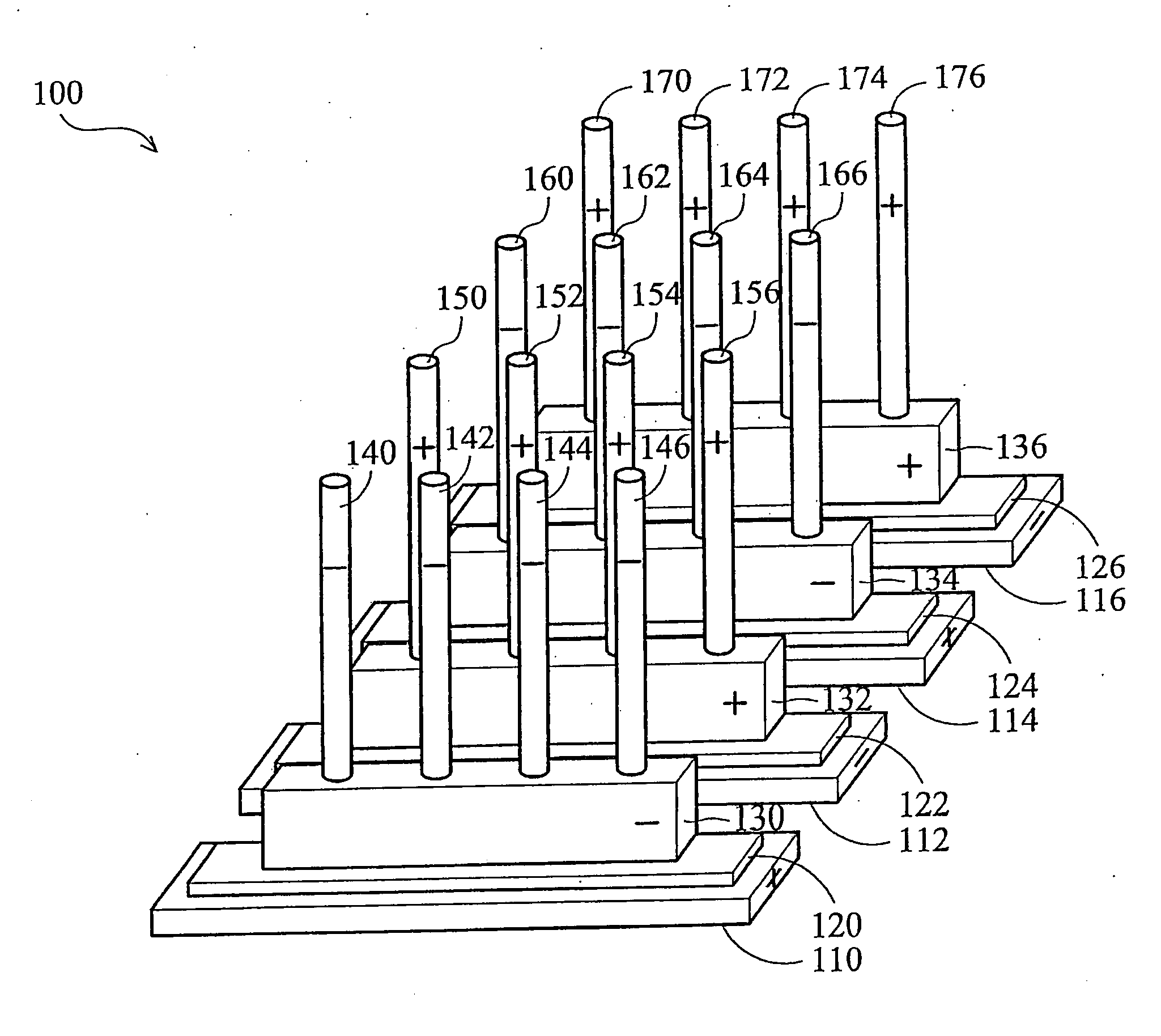
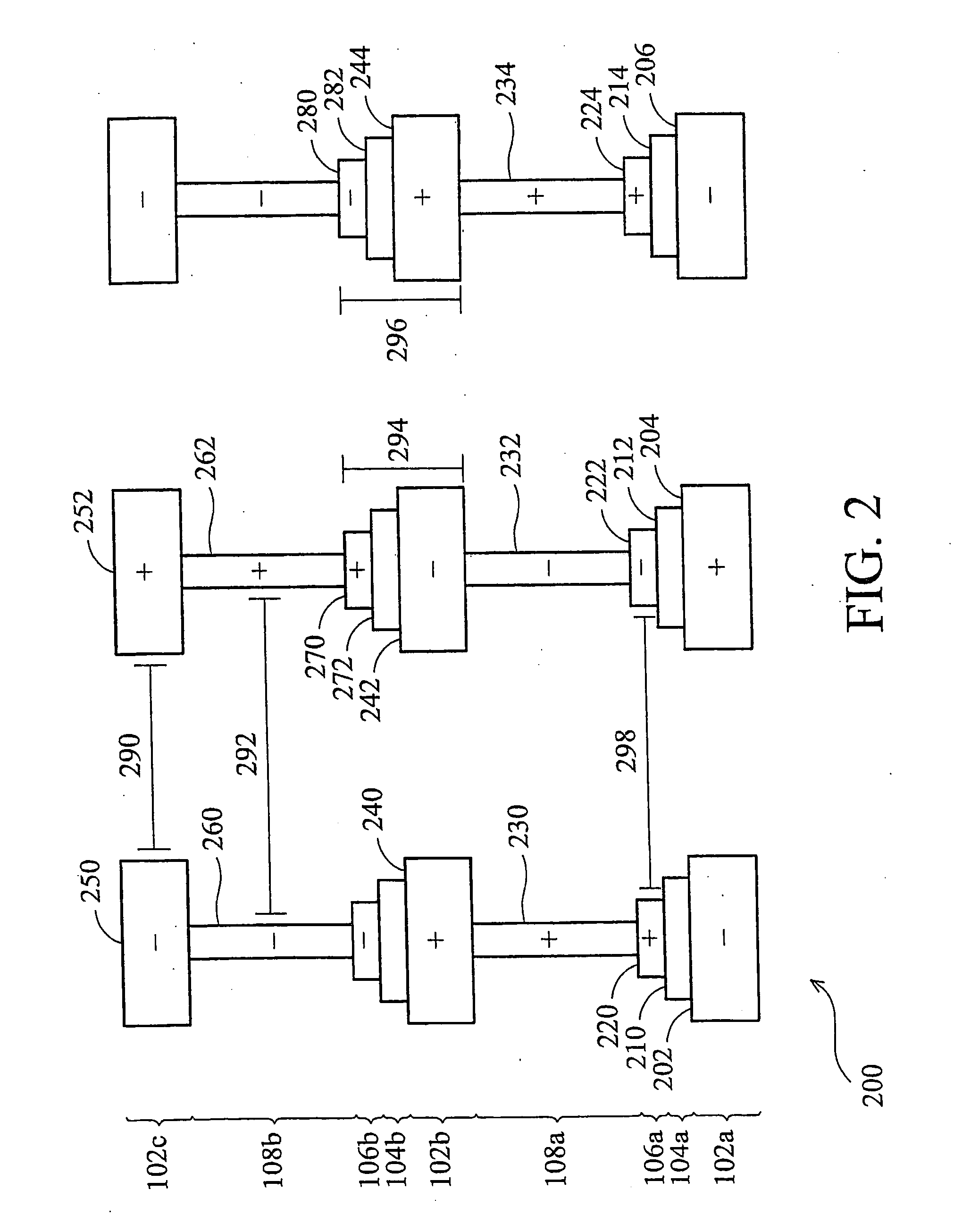
[0025] With reference now to FIG. 1, there is shown a schematic cross sectional view of a capacitive structure for an integrated ...


PUM


Abstract

System and method for an improved interdigitated capacitive structure for an integrated circuit. A preferred embodiment comprises a first layer of a sequence of substantially parallel interdigitated strips, each strip of either a first polarity or a second polarity, the sequence alternating between a strip of the first polarity and a strip of the second polarity. A first dielectric layer is deposited over each strip of the first layer of strips. A first extension layer of a sequence of substantially interdigitated extension strips is deposited over the first dielectric layer, each extension strip deposited over a strip of the first layer of the opposite polarity. A first sequence of vias is coupled to the first extension layer, each via deposited over an extension strip of the same polarity. A second layer of a sequence of substantially parallel interdigitated strips can be coupled to the first sequence of vias.

Description

TECHNICAL FIELD [0001] The present invention relates generally to capacitors for integrated circuits, and more particularly to system and method for an improved interdigitated capacitive structure for an integrated circuit. BACKGROUND [0002] Generally, capacitors are employed in integrated circuits to perform a variety of functions. Capacitors can be used to construct band pass filters, phase locked loops (PLLs), dynamic random access memory (DRAM) components, and a host of other useful devices. In some instances, some common elements of an integrated circuit exhibit inherent capacitance. [0003] For example, certain active integrated circuit elements, such as, for example, bipolar and metal-oxide-semiconductor (MOS) transistors, contain electrical junctions that exhibit capacitance. In fact, depending on the particular type of transistor, a depletion region of an electrical junction can be described as functionally equivalent to a small parallel-plate capacitor. Such a capacitor can...

Claims


Application Information

Patent Timeline
IPC IPC(8): H01L29/00
CPCH01L23/5223H01L28/60H01L2924/0002H01L2924/00H10B99/00H10B12/00
Inventor CHEN, YUEH-YOUCHANG, CHUNG-LONGCHAO, CHIH-PING
Owner TAIWAN SEMICON MFG CO LTD
Why Eureka
Eureka Blog
Learn More